
 Worksheets
Chujowy egzamin 1
Total questions: 15
Worksheet time: 3hrs 30mins
The series resistance of a semiconductor diode in room temperature depends on:
the length of p and n materials
temperature
cross section area of the p and n n materials
current Id flowing through it
doping
concentration of the p and n materials

what is the absolute value of the current flowing through the resistor R2, if Uin = -10V, R1 = 0,5kOhm, R2 = 3kOhm, Udz = 3V
2mA
0mA
3mA
0,7mA
1mA
after applying a constant voltage to a two terminal component made of a p - doped silicon:
there will flow a drift current
there will flow a diffusion current
there will be no current
there will flow both diffusion and drift currents
pytanie4 - brak odp
a
a
a
A cubic 1 cm^3, made of intrinsic silicon, after introducing donor dopant
will be negatively charged
will have more electrons than holes
will behave electrically indifferent
will be positively charged
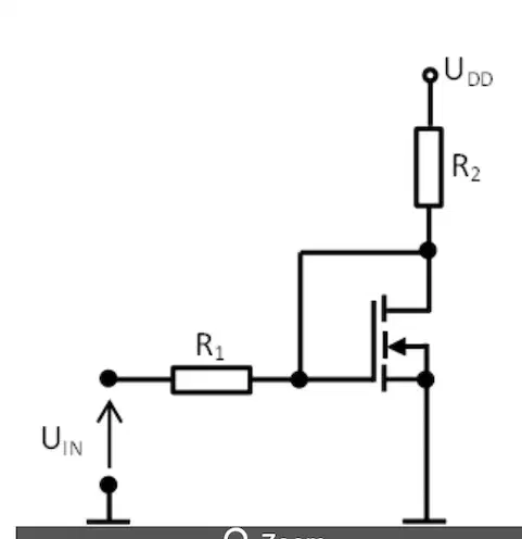
A circuit with enhanced n - MOS transistor is given.
What is the value of the current IR2 flowing through the resistor R2 , if R2=103 Ω , measured VGS = +3V , UDD = +5V, UTH = 2V(threshold voltage)
Brak odpowiedzi!
I_R2 = 1 mA
I_R2 = 3 mA
I_R2 = 2 mA
I_R2 = 0 mA
I_R2 = 4 mA
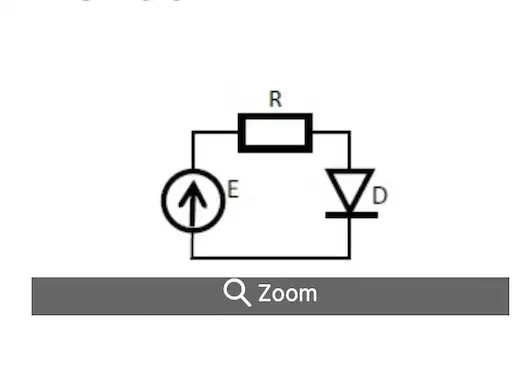
In the following circuit E = 7V, R = 1kOhm and the forward bias diode voltage is 0,7V at the temp 20*C. By how much the current will change if the temperature increases to 50*C
it will increase by 60μA
it will decrease by 60μA
it will decrease by 100μA
it will increase by 100μA
it will stay the same
pyt 8 - brak
a
a
9 - brak odp
a
a

In the following circuit E1 = -5V, E2 = -10V, Re = 10kOhm, Rc = 1kOhm, β=100 . What is the operating state of the BJT
Active inverse
active normal
saturation
can't be estimated
cut - off

In semiconductor technology the BRIDGAMS' horizontal method is used in:
doping process
fabrication of three material npn or pnp structures of BJTs
creating the junctions
in the last stage of the MOS transistors fabrication processes
forming crystals from poly crystals
In the 2D energy band model of semiconductor materials the Fermi level depends on
semiconductor material
current
voltage
dopant concentration
geometrical dimensions of the material
after applying a sine wave voltage to a two terminal component made of n doped silicon
there will flow a current both in forward and reverse direction
there will flow a current if only the voltage exceeds 0,7V
there will flow a current only in forward direction
there will flow a current only in reverse direction

A
B
C
D
G
Which is true?
semiconductor materials in Zener diode Udz = 3V are more doped than in a zener diode Udz = 7V
semiconductor materials in tunneling diode are more doped than in a zener diode Udz = 5V
semiconductor materials in Zener diode Udz = 3V are more doped than in a zener diode Udz = 5V
semiconductor materials in tunneling diode are less doped than in a zener diode Udz = 10V

