
Font size
 Worksheets
Introduction to Digital IC
Total questions: 69
Worksheet time: 12mins
Which company invented the first microprocessor in 1971?
Microsoft
Apple
Intel
Texas Instruments

Identify this computer component:
Transistor
Integrated Circuit (IC)
Microprocessor
Vacuum Tube
It was the first microprocessor introduced by Intel Corporation.
4004 Chip
CPU
Microprocessor
In MOS transistors, _____ is used for their gate
Metal
Silicon di Oxide
Source/Drain
Polysilicon
Source in nMOS transistors is doped with ______ material
p-type
n-type
both n and p-type
Neither n or p-type
During the fabrication process the photoresist layer is exposed to
visible light
ultraviolet light
infra red light
LED
The condition for linear region is
Vgs lesser than Vt
Vgs greater than Vt
Vds lesser than Vgs
Vds greater than Vgs
What is the channel length modulation effect?
Ids decreases with Vds
Ids increases with Vds
Ids is constant with increasing Vds
Which type of technology has a higher cost per piece?
FPGA
ASIC
Custom ASIC
Intel currently has a CMOS technology process in which λ = 11 nm. What is the minimum size of the transistor?
11 nm
22 nm
33 nm
44 nm
What are the advantages of Moore's Law?
More functions can be integrated on single chip
Cost decreases by 2x
Transistors can switch at a faster rate
Chips have lower temperatures
What are the advantages of smaller transistor sizes?
Lower cost
More transistors per unit area
Faster switching speeds
Higher current
Higher gate voltage
Which model is used for scaling?
constant electric scaling
constant voltage scaling
constant electric and voltage scaling
constant current model
Regularity is the ratio of
total transistors in the chip to total transistors that must be designed in detail
total transistors that must be designed in detail to total transistors in chip
total transistors to total components
total charge storage components to charge dissipating components

In the graph, the regions marked as A,B,C are
A : Saturation, B : Linear, C : Cut-off
A :Cut-off, B : Linear, C : Saturation
A : Linear, B : Saturation, C : Cut-off
None of the mentioned
How is nMOS depletion mode transistor represented?


Which model is used for scaling?
a) constant electric scaling
b) constant voltage scaling
c) constant electric and voltage scaling
d) constant current model
The ______ is used to reduce the resistivity of poly silicon.
a) Photo resist
b) Etching
c) Doping impurities
d) None of the mentioned
Which color is used for n-diffusion in stick diagram?
a) red
b) blue
c) green
d) yellow

The output F of the shown 4 to 1 Multiplexer is
XY
X+Y
X+Y
XY

The NMOS circuit chain shown in the figure can act as a
Buffer
NAND Gate
NOR Gate
Invertor
The fastest logic family is
CMOS
NMOS
TTL
ECL
Supply voltage of a CMOS circuit is doubled. Its dynamic power dissipation will
not change
be doubled
be halved
increase by 4 times
Silicon oxide is patterned on a substrate using:
Physical lithography
Chemical lithography
photolithography
none of these
As channel length becomes smaller
a. Longitudinal electric field component Ey reduces
b. Longitudinal electric field component Ey remains same
c. Longitudinal electric field component Ey increases
d. None of the above
When the MOSFET is in depletion mode, the MOS capacitance is
a. Oxide capacitance
b. Depletion layer capacitance
c. Series combination of oxide capacitance and depletion layer capacitance
d. Parallel combination of oxide capacitance and depletion layer capacitance
The VLSI design flow starts with:
RTL synthesis
Product specifications
Library mapping
What is the purpose of function verification?
for debugging
prove the structural netlist perform the same function as the original behavior HDL
to check the speed performance
What is design flow?
A set of procedure that allows designers to progress from a specification for a chip to the final chip implementation in an error-free way
A set of procedure that allows designers to progress from a specification for a chip to the final chip implementation in an error way
The active components in an ICs are
Resistors
capacitors
Diodes and transistors
None of above
In Very large scale Integration VLSI,No of components integrated on same chip are
less than 100
more than 100
more than 1000
less than 1000
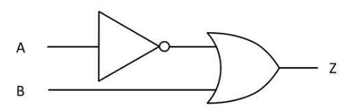
What is the Logic Expression for this circuit?
Z = NOT (A AND B)
Z = NOT (A OR B)
Z = (NOT A) AND B
Z = (NOT A) OR B
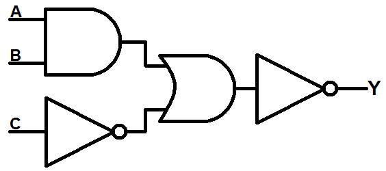
What is the output Y of this logic cricuit if A = 1, B = 1, and C = 1
0
1
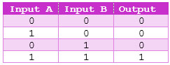
Which logic gate is represented by this truth table?
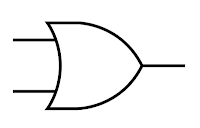
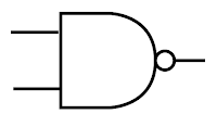
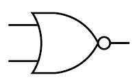

By making them practical, who is widely regarded as the father of modern ICs?
Jack Kilby
Robert Noyce
Sherman Fairchild
Gordon Moore

The starting material for making integrated circuits is a slice of silicon called ___
a cookie
a wafer
a biscuit
a cracker

Which type of layer is added on top of the silicon to act as a protective coating?
a thin oxide layer
a photoresist
a photo mask
phosphorus

Which layer, when exposed to light, becomes soluble so it can be washed away?
a thin oxide layer
a photoresist
a photo mask
phosphorus

Which process uses a high temperature gas, like phosphorus, to change the conductivity of silicon?
doping
debasing
injection molding
narcotizing

Which process deposits a thin layer of metal, like aluminum or copper, onto the wafer?
doping
oxide lithography
etching
metalization

We can focus a ______ onto a very small patch of silicon, creating incredibly fine details
thin oxide layer
photo resist
photomask
microchip

In 1968, Noyce and Moore teamed up and founded a new company, the largest chip maker today: ___
NVIDIA
Qualcomm
Texas Instruments
Intel

How many transistors were contained in the Intel 4004 CPU, the first microprocessor?
23
230
2,300
23,000

In what year did the transistor count in a CPU breach one billion?
1980
1990
2000
2010
Advantages of IC over Discrete Component
Provides signal and power distribution.
Provides mechanical support.
Low power consumption
Draws heat away from the Chip
Functions of Integrated Circuit (IC) packages?
Very Low Weight
High reliability
Easy replacement
Draws heat away from the Chip
Etching is used for:
Selective removal of the unwanted surface
Cleaning
Interconnection
Protection
Which one of the following is not commonly used for deposition of films in Microelectronic devices processing
Polysilicon
Polyethylene
Silicon nitride
Silicon dioxide
Most widely used oxide in IC technology today is
Aluminium oxide
Silicon nitride
Carbon dioxide
Silicon dioxide
The process by which the geometric patterns that define devices are transferred to the substrate surface are is called as
Calligraphy
Lithography
Photography
Oxidation
The main drawback of Electron-beam and Ion-beam lithography is
less scan time
low resolution than photolithography
low current density
beams have to be maintained in a vacuum
For wire bonding , the wires were made of
Gold
Platinum
Copper
Silver
Which of the following is the fastest, smallest, and cheapest per unit to implement a given complex circuit in large volume?
FPGA
ASIC
PLA
CPLD
What are the advantages of smaller transistor sizes?
Lower switching speeds
Higher current
More transistors per unit area
Higher gate voltage

Bonding Pad of IC show in ______________
A
B
C
D
N-well is formed by ______
Decomposition
Diffusion
Dispersion
Filtering
In nMOS device, gate material could be ____________
Silicon
Polysilicon
Boron
Phosphorus
Stick diagrams are those which convey layer information through
Thickness
Color
Shape
Layers
nMOS devices are formed in _________
p-type substrate of high doping level
n-type substrate of low doping level
p-type substrate of moderate doping level
n-type substrate of high doping level
____ technology is preferred than________ technology
NMOS,PMOS
PMOS,NMOS
NMOS,CMOS
PMOS,CMOS
Few parts of photoresist layer is removed by using _________
Acidic Solution
Neutral Solution
Pure Water
Diluted Water
What significant advancement in electronics occurred in 1947 at Bell Labs?
Invention of the vacuum tube
Invention of the transistor
Development of the microprocessor
Introduction of integrated circuits
Which innovation by Jack Kilby in 1958 revolutionized electronics manufacturing?
Transistor
Vacuum tube
Microprocessor
Integrated circuit (IC)
What was the primary motivation for developing the Intel 4004 microprocessor in 1971?
To power early personal computers
To revolutionize telecommunications
To create advanced gaming consoles
To build calculators
What did Gordon Moore's observation in 1965, known as Moore's Law, state?
The number of transistors on a chip doubles approximately every two years.
The speed of microprocessors increases linearly over time.
The cost of integrated circuits decreases exponentially.
The size of vacuum tubes remains constant.
Which microprocessor introduced the x86 architecture and its 16-bit design?
Intel 4004
Intel 8080
Intel 8086
Intel 8008
What was the key advancement introduced by the Pentium series of microprocessors in 1993?
Superscalar architecture
32-bit processing
Reduced power consumption
Compatibility with vacuum tubes
Which microprocessor architecture could address a memory system of 16M bytes?
Intel 8086
Intel 80286
Intel 8080
Intel 4004
What was the primary reason for the introduction of the 80286 microprocessor in 1983?
To address the limitations of a 1M-byte memory system
To replace the 8086 microprocessor
To create a more energy-efficient microprocessor
To focus on instruction simplification

