
 Worksheets
REVIEW ACDC
Total questions: 78
Worksheet time: 55mins
Potential difference between two test points resulting from the distribution of charge in
the circuit.
(a)
6 Known Methods of Producing a Voltage.
(a)
voltage produced by rubbing a certain
material together
Friction
Pressure
Heat (Thermoelectricity)
Light (Photoelectricity)
Chemical Action
Voltage produced by
heating the joint (junction) where two unlike
metals are joined.
Heat
Pressure
Magnetism
Light (Photoelectricity)
Chemical Action
voltage produced by squeezing
crystals of certain substances
Friction
Pressure
Heat (Thermoelectricity)
Magnetism
Chemical Action
Voltage produced by
light striking photosensitive substances.
Friction
Light (Photoelectricity)
Heat (Thermoelectricity)
Magnetism
Chemical Action
Voltage produced by
chemical reaction in a battery cell.
Friction
Light (Photoelectricity)
Heat (Thermoelectricity)
Magnetism
Chemical Action
Produced when conductor moves
to a magnetic field, cutting the magnetic lines of
force of the field.
Friction
Light (Photoelectricity)
Heat (Thermoelectricity)
Magnetism
Chemical Action
Net amount of charge flowing past a
specified point measured in Amperes.
POWER
CURRENT
VOLTAGE
Energy given in a certain amount of time,
usually measured in Watts.
POWER
CURRENT
VOLTAGE
“A current of one amp means that in one second
about _____electrons move through a cross
section of conductor.
6.24x10^18
3.24x10^18
6.24x10^15
3.24x10^15
rate at which electrical energy is
expended or used up or the rate of electric energy
converted into another form.
(a)
Device that limits the flow of electrons through a
circuit.
(a)
Variable resistors
(a)
Potentiometer - __ TERMINALS
3
2
1
Rheostat - __ TERMINALS
3
2
1
used for one-time adjustment
(single turn or multiple turn)
POTENTIOMETER
RHEOSTAT
TRIMMER
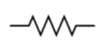
FIXED RESISTOR
RHEOSTAT
POTENTIOMETER
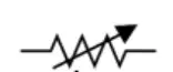
FIXED RESISTOR
RHEOSTAT
POTENTIOMETER

FIXED RESISTOR
RHEOSTAT
POTENTIOMETER
magnitude of the direct opposition to
current
Resistance
Tolerance
Derating Factor
Critical Resistance
Taper
resistance value where the
maximum voltage and power rating occurs
Resistance
Tolerance
Derating Factor
Critical Resistance
Taper
Represents Minimum and Maximum
variation of resistance from its rated value.
Power Rating
Tolerance
Derating Factor
Drift
Wiper or Slider Current
refers to the change in resistance with time
(time stability)
Power Rating
Tolerance
Derating Factor
Drift
Wiper or Slider Current
maximum continuous power that
the resistor can dissipate
Power Rating
Taper
Derating Factor
Drift
Wiper or Slider Current
indicates how the power rating of
the resistor decreases as temperature increases.
Power Rating
Taper
Derating Factor
Drift
Wiper or Slider Current
for variable resistors, this is the variation of
resistance as a function of rotation
Power Rating
Taper
Derating Factor
Drift
Wiper or Slider Current
the maximum current that
the wiper can handle.
Power Rating
Taper
Derating Factor
Drift
Wiper or Slider Current
passive electrical component
consisting of a coil of wire which is designed to take
advantage of the relationship between magnetism
and electricity as a result of an electric current
passing through the coil.
(a)
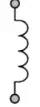
AIR CORE
IRON CORE
FERRITE CORE
VARIABLE CORE
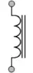
AIR CORE
IRON CORE
FERRITE CORE
VARIABLE CORE

AIR CORE
IRON CORE
FERRITE CORE
VARIABLE CORE
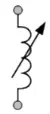
AIR CORE
IRON CORE
FERRITE CORE
VARIABLE CORE
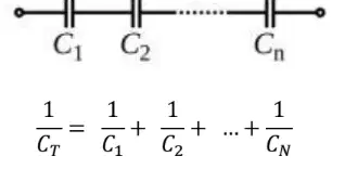
SERIES
PARALLEL
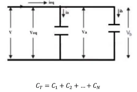
SERIES
PARALLEL
ability of an inductor to resist changes
in current.
(a)
SI UNIT OF INDUCTANCE
(a)
A device used to store an electric charge,
consisting of one or more pairs of conductors
separated by an insulator.
(a)
is the electrical property of a
capacitor and is the measure of a capacitors ability
to store an electrical charge onto its two plates
(a)
is also the property of a capacitor
which resists the change of voltage across it.
(a)
Combination of two or more similar cells, a cell
being the fundamental source of electrical energy
developed through the conversion of chemical or
solar energy
(a)
Division of cells:
(a)
Designed to be used once and discarded
Electrochemical reaction occurring in the cell
is not reversible
PRIMARY CELLS
SECONDARY CELLS
Type of cell which can be charged,
discharged into a load, and recharged many
times
PRIMARY CELLS
SECONDARY CELLS
A junction in a circuit where two or more
circuit elements and/or branches are connected
together.
NODE
BRANCH
LOOP
MESH
Part of a network which lies between two
junctions.
NODE
BRANCH
LOOP
MESH
A closed path in a circuit in which no
element or node is encountered more than once.
NODE
BRANCH
LOOP
MESH
A loop that contains no other loop within it.
NODE
BRANCH
LOOP
MESH
A ______ represents the single circuit
elements like resistor, capacitor, inductor, voltage,
or current source.
NODE
BRANCH
LOOP
MESH
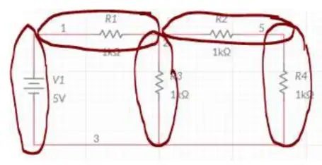
represents the single circuit
elements like resistor, capacitor, inductor, voltage,
or current source.
NODE
BRANCH
LOOP
MESH
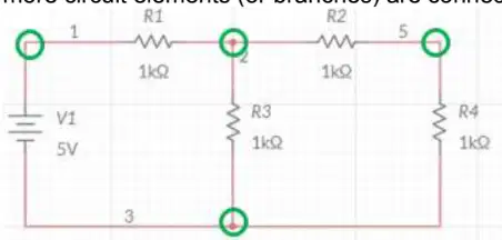
a point in the circuit where two or
more circuit elements (or branches) are connected.
NODE
JUNCTION
LOOP
MESH
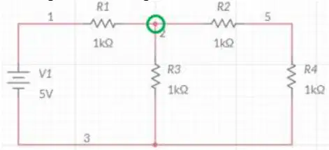
a specific type of node where three or more
components or conductors meet. It is a point of
convergence or divergence within a circuit.
NODE
JUNCTION
LOOP
MESH
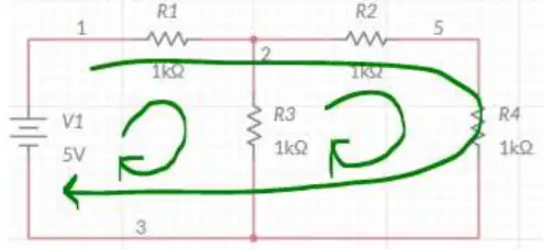
Any closed path in the circuit is called as a
______. A ____ is a closed path formed by starting at a
node, passing through a set of nodes, and returning
to the starting node without passing through any
node more than once.
NODE
JUNCTION
LOOP
MESH
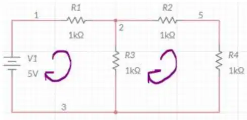
is a closed path in the circuit, which
does not contain any other close path inside it.
NODE
JUNCTION
LOOP
MESH
-One of the most fundamental law in
electrical circuits relating voltage, current and
resistance.
(a)
I = E/R
(a)
More comprehensive than Ohm’s Law and is
used in solving electrical networks
Termed as Law of Electric Networks
Formulated by German physicist Gustav Robert
Kirchhoff
(a)
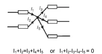
“In any electrical network, the algebraic sum
of the current meeting at a point (or a junction) is
zero.”
(a)
(a)
“The algebraic sum of the products
and resistances in each of the conductors in any
closed path in a network plus the algebraic sum of
the emf’s in that path is zero.”
(a)
elements which conduct electricity
very readily
Conductors
Electrical Conductors
Insulators
Electrical Insulators
Semiconductors
– are materials that allow the
essentially free passage of current when connected
to a battery or other source of electrical energy,
_______ have 3 or less valence electrons
Exhibit positive temperature coefficient
Silver is the best conductor
Conductors
Electrical Conductors
Insulators
Electrical Insulators
Semiconductors
have an extremely high resistance to
the flow of electricity
Electrical Semiconductors
Electrical Conductors
Insulators
Electrical Insulators
Semiconductors
– are materials that doesn’t
allow/oppose free passage of current
_____ have 5 or more valence electrons
______ exhibits Negative Temperature Coefficient
Examples are plastic, rubber and dry wood.
Electrical Semiconductors
Electrical Conductors
Insulators
Electrical Insulators
Semiconductors
All matter between insulator
and conductor
Electrical Semiconductors
Electrical Conductors
Insulators
Electrical Insulators
Semiconductors
are materials that have
conductivity about midway between conductors and
insulators.
______ have 4 valence electrons
Examples are Silicon and Germanium.
Electrical Semiconductors
Electrical Conductors
Insulators
Electrical Insulators
Semiconductors
A diode designed to operate in the reverse
breakdown region
Application: voltage regulator
Biasing: Reverse Bias
(a)
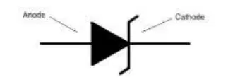
Characteristics:
Semiconductor device that permits current
to flow in either a forward or reverse
direction.
The diode consists of a special, heavily
doped p-n junction, designed to conduct in
the reverse direction when a certain
specified voltage is reached.
(a)
a diode that always operates in
reverse bias and is doped to maximize the inherent
capacitance of the depletion region.
Application:
Variable Capacitor – Tuned Circuits
: Reverse Bias
(a)
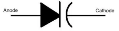
Characteristics:
The diode whose internal capacitance
varies with the variation of the reverse
voltage.
It is used for storing the charge.
Always works in reverse bias, and it is a
voltage-dependent semiconductor device
(a)
Also known as Hot - Carrier Diode
Forms a metal to semiconductor junction
Application: High-Frequency and Fast Switching
Biasing: Reverse Bias
(a)
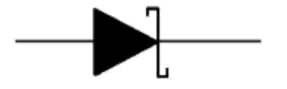
Characteristics:
Metal-semiconductor diode with a low forward
voltage drop and a very fast switching speed
Unlike a conventional pn-junction diode which is
formed from a piece of P-type material and a
piece of N-type material, (a) are
constructed using a metal electrode bonded to
an N-type semiconductor.
Used in high frequency and fast switching
applications.
Schottky diode’s recovery time ranges from
____ to tens of nanoseconds.
A typical p-n diode has a recovery time of several
_____
(a)
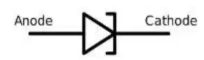
Characteristics:
Also known as Esaki diode.
Type of diode that exhibits the phenomenon
known as negative resistance. When
voltage value increases, current flow
decreases.
A _________ is a heavily doped p-n
junction diode.
______ works based on _____ Effect.
(a)
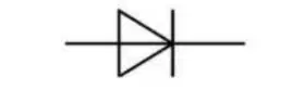
diode is a one type of photo detector, used to
convert optical signal into an electrical signal. The
PIN diode comprises of three regions, namely P-
region, I-region and N-region.
P-type layer
Intrinsic layer
N-type layer
(a)
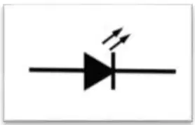
Characteristics:
Is a pn junction device that emits light when
forward biased
Are semiconductor light sources that
combine a P-type semiconductor (larger
hole concentration) with an N-type semiconductor (larger electron
concentration).
(a)
(a) wavelengths are in-phase with
respect to space and time. (LEDs emit non-
coherent light)
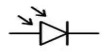
Characteristics:
A device that operates in the reversed bias.
A device that is built to increases its leakage
current when it is exposed to light.
(a)

