
 Worksheets
AMC_Quiz
Total questions: 5
Worksheet time: 8mins
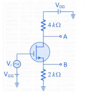
Consider the circuit shown with an ideal nMOSFET. The transistor is appropriately biased in the saturation region with VGG and VDD such that it acts as a linear amplifier. vi is the small-signal ac input voltage. vA and vB represent the small-signal voltages at the nodes A and B, respectively. The value of VBVA is __________
-2
2
-4
4
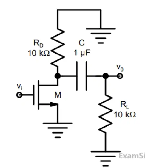
The ac schematic of an NMOS common-source stage is shown in the figure below, where part of the biasing circuits has been omitted for simplicity. For the n -channel MOSFET M, the transconductance gm = 1 mA/V, and body effect and channel length modulation effect are to be neglected. The lower cutoff frequency in Hz of the circuit is approximately at
8
32
50
200
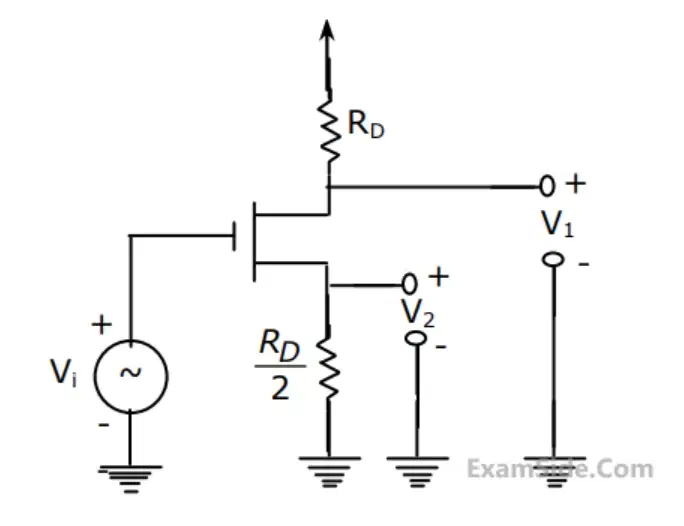
In the MOSFET amplifier of the figure the signal output V1 and V2 obey the relationship
V1 = V2/2
V1 = - V2/2
V1=2V2
V1= -2V2
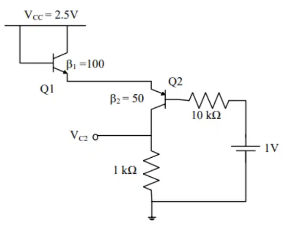
Consider the circuit shown in the figure. Assuming VBE1 = VEB2 = 0.7 volt, value of the dc voltage Vc2 (in volt) is _______
0.5 V
0.52V
1V
1.5V
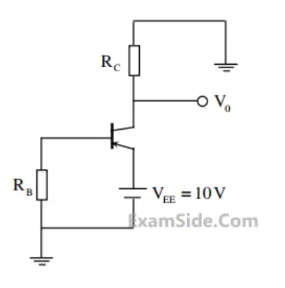
In the circuit shown, the PNP transistor has |VBE|=0.7V and β = 50. Assume that RB = 100 kΩ. For V0 to be 5 V, the value of RC ( in kΩ) is _____________.
1.07K ohm
1k ohm
1.1k ohm
1.5k ohm

