
 Worksheets
ICE ELECS 3 (Electronics Devices and Circuits Theory 2)
Total questions: 200
Worksheet time: 2hrs 40mins
Which of the following ratings is true?
Si diodes have lower PIV and narrower temperature ranges than Ge diodes.
Si diodes have lower PIV and wider temperature ranges than Ge diodes.
Si diodes have higher PIV and wider temperature ranges than Ge diodes.
Si diodes have higher PIV and narrower temperature ranges than Ge diodes.
Which capacitance dominates in the reverse-bias region?
conversion
None of the above
Diffusion
depletion
What unit is used to represent the level of a diode forward current IF?
uA
nA
mA
pA
The diffused impurities with ________ valence electrons are called donor atoms.
0
5
4
3
What is the range of the operating voltage level for LEDs?
1.7–3.3 V
5–12 V
5–12 mV
20–25 V
At what kind of operating frequency diffusion or transition is a capacitor represented in parallel with the ideal diode?
Mid frequency
Moderate frequency
Very high frequency
Low frequency
What is the resistor value of an ideal diode in the region of conduction?
Undefined
5k
0
Infinity
Calculate the power dissipation of a diode having ID = 40 mA.
28 mW
28 W
280 mW
Undefined
In which of the following is the light intensity measured?
Flux
Candela
Illumination
Efficacy
Calculate the temperature coefficient in %/°C of a 10-V nominal Zener diode at 25°C if the nominal voltage is 10.2 V at 100°C.
0.0267
0.0321
0.0251
0.0238
A silicon diode has a voltage to ground of –117 V from the anode. The voltage to ground from the cathode is –117.7 V. The diode is
shorted.
forward-biased.
reverse-biased.
open.
What is the value of the transition capacitance for a silicon diode when VD = 0? (Choose the best answer.)
5 pF
10 pF
3 pF
1 pF
What type of diode circuit is used to clip off portions of signal voltages above or below certain levels?
none of the above
IC voltage regulator
clipper or limiter
clamper
The output frequency of a full-wave rectifier is ________ the input frequency.
equal to
one-quarter
one-half
twice
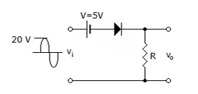
Determine the peak value of the output waveform.
–15 V
25 V
–25 V
15 V
What is the VRRM (PIV rating) for the 1N4001 rectifier diode?
50 V
100 V
400 V
200 V
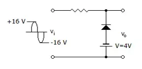
Determine the peak for both half cycles of the output waveform.
16 V, –4 V
–16 V, 4 V
–16 V, –4 V
16 V, 4 V
In a regulated supply, what term describes how much change occurs in the output voltage over a certain range of load current values, from minimum to maximum current?
voltage regulator
load regulation
line regulation
current regulator
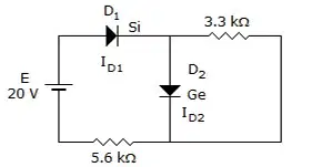
Determine ID2.
3.393 mA
6.061 mA
0.7 mA
3.571 mA
What is the PIV for each diode in a full-wave center-tapped rectifier? Note: Vp(out) = peak output voltage.
Vp(out) + 0.7 V
2Vp(out) – 0.7 V
2Vp(out) + 0.7 V
Vp(out) – 0.7 V
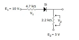
Determine V2.
1.371 V
4.3
0 V
3.201
How many terminals do the 7800 series fixed positive voltage regulators have?
3
2
4
5
A silicon diode in a half-wave rectifier has a barrier potential of 0.7 V. This has the effect of
increasing the peak output voltage by 0.7 V.
no effect.
reducing the peak output voltage by 0.7 V.
reducing the peak input voltage by 0.7 V.
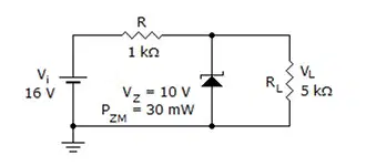
Calculate IL and IZ.
2 mA, 4 mA
2 mA, 0 mA
2 mA, 2 mA
4 mA, 2 mA
In a particular problem, which mode has the highest level of IDQ?
Ideal
Approximate equivalent
None of the above
Exact mode using characteristic curve
In the operation of a half-wave rectifier with a capacitor-input filter, the ripple factor can be lowered by ________ the value of the filter capacitor or ________ the load resistors.
increasing, decreasing
decreasing, increasing
decreasing, decreasing
increasing, increasing
A diode is in the "________" state if the current established by the applied sources is such that its direction matches that of the arrow in the diode symbol, and VD ≥ 0.7 V for Si and VD ≥ 0.3 V for Ge.
quiescent
on
neutral
off
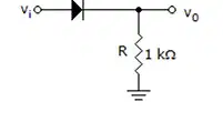
What best describes the circuit?
Half-wave rectifier
Clamper
Full-wave rectifier
Clipper
What is the maximum power rating for LEDs?
500 mW
10 W
1 W
150 mW
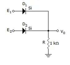
What is the logic function of this circuit?
Negative logic OR gate
Positive logic AND gate
Positive logic OR gate
Negative logic AND gate
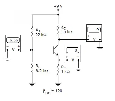
Refer to the given figure. The most probable cause of trouble, if any, from these voltage measurements is
a short from collector to emitter.
the base-emitter junction is open.
RE is open.
no problems.
Which transistor bias circuit provides good Q-point stability with a single-polarity supply voltage?
emitter bias
voltage-divider bias
collector-feedback bias
base bias
Emitter bias requires
no supply voltage.
only a positive supply voltage.
both positive and negative supply voltages.
only a negative supply voltage.
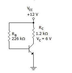
Refer to this figure. The value of IB is
53 uA.
50 uA.
53 mA.
50 mA.
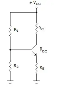
In the voltage-divider biased npn transistor circuit, if R2 opens, the transistor is
nonconducting.
conducting
cutoff.
saturated.
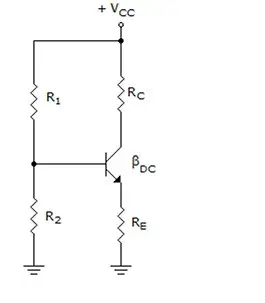
In the voltage-divider biased npn transistor circuit, if RC opens, the transistor is
conducting
saturated.
nonconducting.
cutoff.
Which transistor bias circuit arrangement has poor stability because its Q-point varies widely with BDC?
collector-feedback bias
emitter bias
base bias
voltage-divider bias
At saturation the value of VCE is nearly ________, and IC = ________.
VCC, IC(sat)
VCC, zero
zero, zero
zero, I(sat)
The input resistance of the base of a voltage-divider biased transistor can be neglected
at all times.
only if the base current is much larger than the current through R2 (the lower bias resistor).
only if the base current is much smaller than the current through R2 (the lower bias resistor).
at no time.
Changes in BDC result in changes in
the Q-point.
all of the above
VCE.
IC.
The cutoff region is defined by IB ________ 0 A.
=<
<
>
>=
In a fixed-bias circuit, which one of the stability factors overrides the other factors?
S(VBE)
S(B)
Undefined
S(ICO)
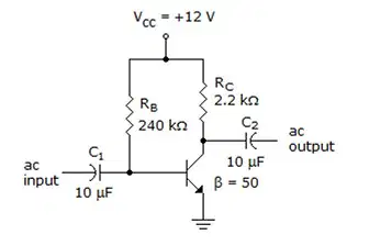
For what value of B does the transistor enter the saturation region?
75
50
20
116
At what region of operation is the base-emitter junction forward biased and the base-collector junction reverse biased?
Saturation
Linear or active
Cutoff
none of the above
Calculate the storage time in a transistor switching network if toff is 56 ns, tf = 14 ns, and tr = 20 ns.
34 ns
42 ns
70 ns
36 ns
Determine ICQ at a temperature of 175ºC if ICQ=2mA at 25º C for RB/RE = 20 due to the S(B) stability factor.
2.58 mA
2.392 mA
2.25 mA
2.417 mA
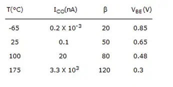
Use this table to determine the change in IC from 25ºC to 175ºC for RB/RE = 250 due to the S(ICO) stability factor. Assume an emitter-bias configuration.
0.14034 nA
42.53 nA
140.34 nA
140.34 uA
For the typical transistor amplifier in the active region, VCE is usually about _______% to ______% of VCC.
30, 70
40, 90
25, 75
10, 60
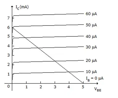
Calculate Rsat in ohms if VCE = 0.3 V.
49.2 m
49.2 M
49.2 k
49.2
Which of the following is (are) the application(s) of a transistor?
Amplification of signal
Computer logic circuitry
All of the above
Switching and control
For the BJT to operate in the saturation region, the base-emitter junction must be ________-biased and the base-collector junction must be ________-biased.
forward, reverse
reverse, reverse
reverse, forward
forward, forward
Which of the following voltages must have a negative level (value) in any npn bias circuit?
None of the above
VCE
VBE
VBC
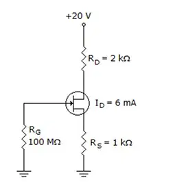
Refer to figure given below. Calculate the value of VDS.
2 V
4 V
–2 V
0 V
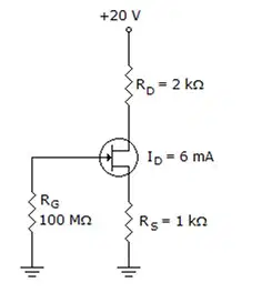
Refer to figure shown below. Determine the value of VS.
2 V
20 V
8 V
6 V
On the drain characteristic curve of a JFET for VGS = 0, the pinch-off voltage is
above the breakdown region.
between the ohmic area and the constant current area.
between the constant current area and the breakdown region.
below the ohmic area.
Which of the following devices has the highest input resistance?
JFET
bipolar junction transistor
diode
MOSFET
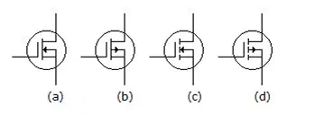
Identify the p-channel D-MOSFET.
a
b
c
d
A dual-gated MOSFET is
either a depletion or an enhancement MOSFET.
a depletion MOSFET.
a VMOSFET.
an enhancement MOSFET.
High input resistance for a JFET is due to
a metal oxide layer.
an intrinsic layer.
the gate-source junction being reverse-biased.
a large input resistor to the device.
For a JFET, the change in drain current for a given change in gate-to-source voltage, with the drain-to-source voltage constant, is
breakdown.
forward transconductance.
reverse transconductance.
self-biasing.
A JFET data sheet specifies VGS(off) = –6 V and IDSS = 8 mA. Find the value of ID when VGS = –3 V.
none of the above
4 mA
2 mA
8 mA
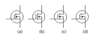
Identify the n-channel E-MOSFET. Use figure at no. 57.
a
b
c
d
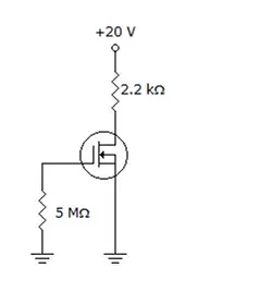
Refer to the given figure. ID = 6 mA. Calculate the value of VDS.
10 V
13.2 V
6.8 V
0 V
The resistance of a JFET biased in the ohmic region is controlled by
VD.
VGS.
VDS.
VS.
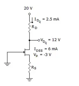
Given the values of VDQ and IDQ for this circuit, determine the required values of RD and RS.
2.5k, 5.3k
3.2k, 400
1k, 5.3k
2k, 2k
The input controlling variable for a(n) ________ is a current level and a voltage level for a(n) ________.
FET, BJT
BJT, BJT
FET, FET
BJT, FET
Through proper design, a ________ can be introduced that will affect the biasing level of a voltage-controlled JFET resistor.
photodiode
laser diode
thermistor
Zener diode
On the universal JFET bias curve, the vertical scale labeled ________ can, in itself, be used to find the solution to ________ configurations.
m, fixed-bias
M, fixed-bias
M, voltage-bias
m, voltage-bias
Which of the following current equations is true?
IG = ID
IG = ID = IS
ID = IS
IG = IS
Which of the following represents the voltage level of VGS in a self-bias configuration?
VGS(off)
VP
VS
VG
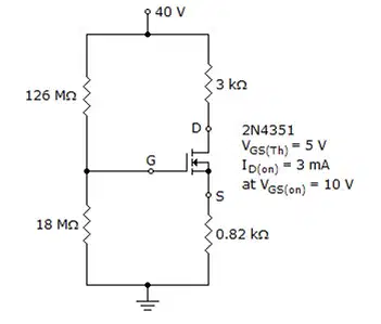
What are the voltages across RD and RS?
20 V, 20 V
10 V, 10 V
5 V, 5 V
0 V, 0 V
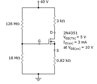
Calculate the value of VDSQ in figure 71 if R1=126MΩ.
40 V
0 V
20 V
30 V
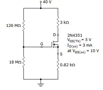
Calculate VD in figure 71 if R1=22MΩ and RS=0.6kΩ.
12.4 V
4.6 V
17.0 V
23.0 V
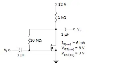
Determine the value of VDSQ.
7.14 V
4.86 V
10 V
3.5 V
Which of the following is a false statement regarding the dc load line when comparing self-bias and voltage-divider configurations?
Both intersect the transfer characteristics.
Both are linear lines.
Both are obtained by writing Kirchhoff's voltage law (KVL) at the input side loop.
Both cross the origin.
For the FET, the relationship between the input and output quantities is ________ due to the ________ term in Shockley's equation.
linear, proportional
linear, squared
nonlinear, cubed
nonlinear, squared
A roll-off of 20 dB per decade is equivalent to a roll-off of ________ per octave.
6 dB
12 dB
3 dB
13 dB
Each RC circuit causes the gain to drop at a rate of ________ dB/decade.
20
10
6
none of the above
Internal transistor junction capacitances affect the high-frequency response of amplifiers by
reducing the amplifier's gain and introducing phase shift as the signal frequency increases.
introducing phase shift as the signal frequency increases.
having no effect.
reducing the amplifier's gain.
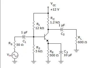
Refer to this figure for 80-83. The capacitor C3 affects
nothing.
high-frequency response.
midrange response.
low-frequency response.
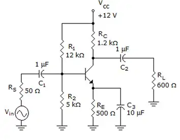
The capacitor Cbe affects
nothing.
high-frequency response.
low-frequency response.
midrange response.
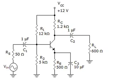
The capacitor C1 affects
high-frequency response.
low-frequency response.
midrange response.
nothing.
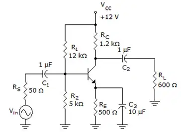
You are attempting to determine the lower cutoff frequency of this amplifier in the lab. As you change the input frequency and measure the output signal, you must remember to
watch for a change of B.
set the oscilloscope to DC
keep a constant temperature.
maintain the input voltage constant.
For low-frequency response, all RC circuits in an amplifier may not have the same critical frequency. Which RC response will determine the critical frequency of the amplifier?
the lowest frequency
bypass frequency
the center frequency
the highest frequency
An amplifier has output voltage of 7.6Vp-p at the midpoint of the frequency range. What is the output at fc?
5.4 V p-p
5.4 Vrms
3.8 Vrms
3.8 V p-p
What term means that the midrange voltage gain is assigned a value of 1 (or 0 dB)?
Miller
corner
critical
normalized
An RC network has values of R = 1.2kΩ and C = 0.22uF. Find fc.
3.79 kHz
60 Hz
603 Hz
1.89 kHz
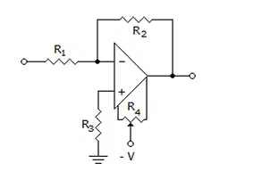
Refer to this figure. The purpose of R3 is
for bias current compensation.
for input offset voltage compensation.
to set input impedance.
to set input impedance and voltage gain.
An op-amp has an open-loop gain of 100,000 and a cutoff frequency of 40 Hz. Find the open-loop gain at a frequency of 30 Hz.
8,000
800
100,000
80,000
An op-amp has an open-loop gain of 75,000 and a cutoff frequency of 100 Hz. At 1 kHz the open-loop gain is down by
3 dB.
20 dB.
10 dB.
6 dB.
The frequency response of an amplifier can be determined using the step response method, and measuring the output rise/fall times between five time constant.
five time constant
25% and 75% response.
0% and 100% response.
10% and 90% response.
What is the difference output voltage of any signals applied to the input terminals?
The common-mode gain times the common input voltage.
The difference of the differential gain times the difference input voltage and the common-mode gain times the common input voltage.
The differential gain times the difference input voltage.
The sum of the differential gain times the difference input voltage and the common-mode gain times the common input voltage.
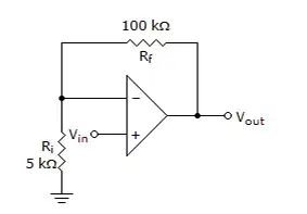
Refer to the given figure. A dc input signal of –50 mV is applied. You would measure ________ from the inverting input to ground.
50 mV
–50 mV
1.05 V
–1.05 V
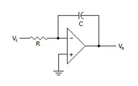
This circuit is referred to as a(n) ________.
noninverting amplifier
differentiator
inverting amplifier
integrator
The purpose of R4 in figure in number 88
to set input impedance.
to set input impedance and voltage gain.
for input offset voltage compensation.
for bias current compensation.
What is the slew rate of an op-amp if the output voltages change from 2 V to 3 V in 0.2 ms?
2 V/ms
3 V/ms
1 V/ms
5 V/ms
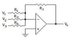
Calculate the output voltage if R1 = R2 = R3 = 100Ω, Rf = 1 kΩ, and V1 = V2 = V3 = 50 mV
0.5 V
–0.5 V
–1.5 V
1.5 V
At what input voltage level does the output voltage level become numerically equal to the value of the differential gain of the amplifier?
Vi1 = –V i2 = 0.75V
Vi1 = –Vi2 = 0.50V
Vi1 = –Vi2 = 0.25V
Vi1 = –Vi2 = 1.00V
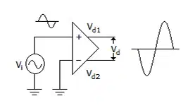
This circuit is an example of a ________.
double-ended output
common-mode operation
double-ended (differential) input
single-ended input
Calculate the output impedance of an inverting op-amp using the 741 op amp (ro = 75Ω, AOL = 200 V/mV) if R1=100Ω and Rf = 1kΩ.
0.375
0.011
0.0375
0.00375
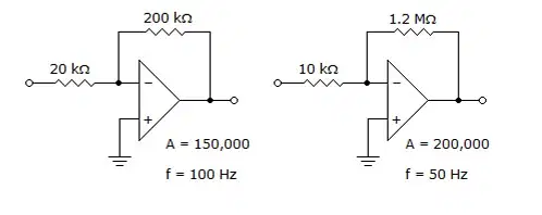
Refer to the given figure. Determine the bandwidth
1.5 kHz
1 MHz
1 kHz
1.5 MHz
Which of the following circuit conditions affect(s) the output offset voltage of an op-amp?
An input offset current, IIO
Both an input offset voltage, VIO and an input offset current, IIO
None of the above
An input offset voltage, VIO
In which of the following operations is the resulting output signal of differential amplifier near zero?
Single-ended
Double-ended
None of the above
Common-mode
Negative feedback added to an op-amp ________ the bandwidth and ________ the gain.
decreases, increases
decreases, decreases
increases, decreases
increases, increases
What is the scale multiplier (factor) of a basic integrator?
–RC
C / R
R / C
–1 / RC
In the differential amplifier circuit, which of the following terminals are connected together?
Emitters
One base to another collector
Collectors
Bases
A(n) ________ amplifier configuration has an input impedance approximately equal to the input resistor Ri and an output impedance approximately equal to the output impedance of the op-amp itself.
non-inverting
differential
inverting
voltage-follower
What is the difference voltage if the inputs are an ideal in-phase signal?
The common-mode gain times the input signal.
The differential gain times the input signal.
The differential gain times twice the input signal.
The common-mode gain times twice the input signal.
The midrange open-loop gain of an op-amp is 135 dB. With negative feedback this gain is reduced to 72 dB. The closed-loop gain is
72 dB.
135 dB.
207 dB.
63 dB.
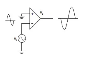
This circuit is an example of a ________.
double-ended output
single-ended input
common-mode operation
double-ended (differential) input
Open-loop voltage gain of an op-amp can range up to ________.
200,000
50,000
100,000
10,000
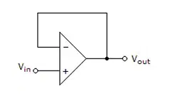
Refer to the given figure. The unity-gain bandwidth of this op-amp is 10.4 kHz.
What is the bandwidth of the circuit?
16.7 kHz
3 MHz
15.5 kHz
10.4 kHz
The voltage gain of a basic instrumentation amplifier is set by a(n)
resistor.
diode.
capacitor.
inductor.
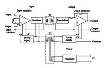
Refer to the given figure. This circuit is a setup for
an antilog amplifier.
an isolation amplifier.
a constant-current source.
a constant-current source.
The main purpose of an instrumentation amplifier is to amplify ________ signals that are riding on ________ common-mode voltages.
small, small
large, small
large, large
small, large
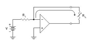
Refer to the given figure. This circuit is a setup for
a constant-current source.
an isolation amplifier.
an antilog amplifier.
an instrumentation amplifier.
A log amplifier may use the ________ junction of a BJT in the feedback loop.
base-collector
base-emitter
base-collector
emitter-ground
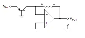
Refer to the given figure. This circuit is a setup for
an antilog amplifier.
an instrumentation amplifier.
an isolation amplifier.
a constant-current source.
e operational transconductance amplifier (OTA) is primarily a ________-to- ________ amplifier.
current, voltage
current, resistance
voltage, current
resistance, current
An antilog amplifier has a ________ in series with the input.
diode or BJT
diode
resistor.
BJT
The process known as signal compression is used with a(n) ____ amplifier.
instrumentation
isolation
antilog
log
The OTA has a ________ input impedance and a ________ CMRR.
high, high
low, low
high, low
low, high
What is a key characteristic of an instrumentation amplifier?
high output offset
none of the above
high output impedance
high CMRR
What part of the characteristic curve of a diode is useful for log amplifiers?
the log region below the zener voltage
the log region above 0.7 V
the log region below 0.7 V
the log region between 0 V and 0.7 V
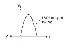
This is an example of the output swing for a class ________ amplifier.
AB
A
C
B
A silicon power transistor is operated with a heat sink (θSA = 1.5ºC/W). The transistor, rated at 150 W (25ºC), has θJC = 0.5º C/W, and the mounting insulation has θCS = 0.6 ºC/W. What is the maximum power that can be dissipated if the ambient temperature is 50ºC and TJmax = 200 ºC?
57.7 W
55.5 W
60.0 W
61.5 W
Class ________ amplifiers are normally operated in a push-pull configuration in order to produce an output that is a replica of the input.
A
B
C
AB
Class AB operation is ________ operation.
similar to class A
similar to class C
similar to class B
None of the above
In class B operation, at what fraction of VCC should the level of VL(p) be to achieve the maximum power dissipated by the output transistor?
0.5
0.636
0.707
1
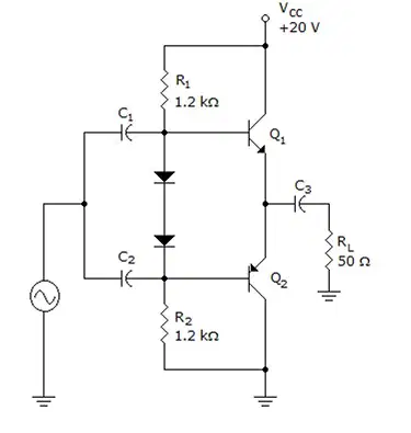
You find that there is an input signal on the base of Q1 and Q2. However, there is no output signal. You then measure the dc voltages on Q2 and find them to be all 0 V. The possible trouble might be
C1 is open.
RL is shorted.
VCC is 0 V.
C3 is shorted.
You have an oscilloscope across RL and it shows a zero signal voltage. The problem might be that
BE2 is open.
R1 is open.
C3 is open.
BE1 is open.
Which of these amplifiers is not intended for large-signal or power amplification?
Class A
Class B or AB
Class D
Class C
Determine what maximum dissipation will be allowed for a 70-W silicon transistor (rated at 25ºC) if derating is required above 25ºC by a derating factor of 0.6 W/ºC at a case temperature of 100º.
25 W
30 W
35 W
40 W
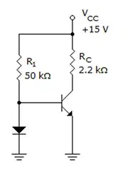
Refer to this figure. This amplifier is operating as a ________ amplifier.
class A
class C
class AB
class B
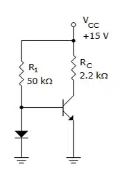
Refer to this figure. The approximate voltages on the base, collector, and emitter, respectively
0 V, 0 V, 0 V.
0.7 V, 0 V, 15 V.
0.7 V, 6.8 V, 0 V.
0.7 V, 15 V, 0 V.
Which amplifier is commonly used as a frequency multiplier?
class B
class C
class A
all of the above
A class B amplifier operates in the linear region for
360° of the input cycle.
much less than 180° of the input cycle.
slightly less than 180° of the input cycle.
slightly more than 180° of the input cycle.
Calculate the efficiency of a transformer-coupled class A amplifier for a supply of 15 V and an output of V(p) = 10 V.
78.5%
25%
50%
33.3%
Categorize the power efficiency of each class of amplifier, from worst to best.
D, B, AB, A
A, B, AB, D
A, AB, B, D
A, AB, D, B
In a class AB amplifier, if the VBE drops are not matched to the diode drops or if the diodes are not in thermal equilibrium with the transistors, this can result in
thermal runaway.
diode separation.
crossover distortion.
a current mirror.
For BJT power transistors, the collector terminal is always connected to the transistor's case
because the collector terminal is the critical terminal for heat dissipation.
to prevent shorts.
because the collector terminal is located nearest the case.
for easy circuit connection.
In practice, the efficiency of a capacitively coupled class A amplifier is about ________%.
40
70
25
10
A class A amplifier with RC = 3.3 kΩ and RE = 1.2 kΩ has a VCC = 20 V. Find IC(sat).
16.7 mA
20 mA
4.4 mA
6.1 mA
Calculate the efficiency of a class B amplifier for a supply voltage of VCC = 20 V with peak output voltage of VL(p) = 18 V. Assume RL = 16Ω.
70.69%
50%
78.54%
75%
Calculate the effective resistance seen looking into the primary of 20:1 transformer connected to 8Ω load.
3.0 kΩ
1.8 kΩ
3.2 kΩ
2.8 kΩ
A class C amplifier has a tank circuit in the output. The amplifier is conducting only 28°. The output voltage is
a sine wave.
a square wave with a frequency determined by the tank.
0 V.
a dc value equal to VCC.
At what phase shift is the magnitude of A at its maximum in the Nyquist plot?
270º
90º
0º
180º
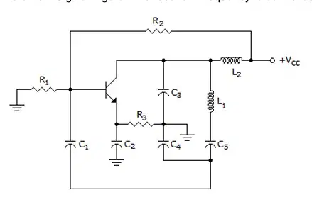
Refer to the given figure. The resonant frequency is controlled by
C2, C4, C5, and L1.
C3 and L1.
C3, C4, C5, and L1.
C3, C4, C5, and L2.
For a phase-shift oscillator, the gain of the amplifier stage must be greater than ________.
29
1
30
19
An amplifier with a gain of –500 and a feedback of B=–0.1 has a gain change of 15% due to temperature. Calculate the change in gain of the feedback amplifier.
0.5%
0.3%
0.4%
0.2%
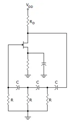
Given gm=5000uS, rd=40kΩ, R=10kΩ, and A=35.
Determine the value of RD for oscillator operation at 1 kHz.
12.3 kΩ
8.48 kΩ
8.05 kΩ
10.8 kΩ
Which of the following is required for oscillation?
BA > 1
Both BA > 1 and the phase shift around the feedback network must be 180º.
The phase shift around the feedback network must be 180º.
None of the above
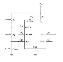
Refer to this figure. This circuit is
a VCO.
a monostable multivibrator.
a sine-wave oscillator.
an astable multivibrator.
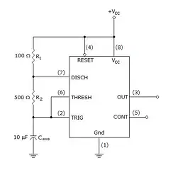
Refer to this figure. Determine the frequency of oscillation, if any.
2.62 kHz
262 Hz
none
131 Hz
What is the ratio of the input impedance with series feedback to that without feedback?
BA
1
B
1 + BA
One condition for positive feedback is that the phase shift around the feedback loop must be ________°.
180
45
90
0
Determine the output impedance with feedback for a voltage-series feedback having A = –100, R1 = 15kΩ, Ro = 20 kΩ, and a feedback of B=–0.25.
392.16Ω
1.82 kΩ
769.23Ω
0.2 kΩ
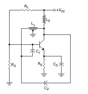
Refer to the given figure. This circuit is known as
an Armstrong oscillator.
Hartley oscillator.
a Clapp oscillator.
a Colpitts oscillator.
In order to start up, a feedback oscillator requires
negative feedback less than 1.
unity feedback equal to 1.
positive feedback greater than 1.
no feedback.
What is the total phase shift requirement, around the feedback loop, for a phase-shift oscillator?
180°
90°
270°
360°
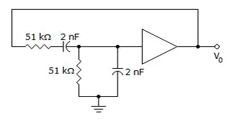
Calculate the resonant frequency of this oscillator.
4681.07 Hz
3120.70 Hz
1560.34 Hz
6241.37 Hz
The lead-lag circuit in the Wien-bridge oscillator has a resonant frequency at which the attenuation is
1/3.
1/5.
1/4.
1/2.
At series resonance, the impedance of a crystal is
minimum.
zero.
equal.
maximum.
The twin-T oscillator produces a ________ response.
low-pass
band-pass
band-stop
high-pass
What is the typical value of quality factor for crystal oscillators?
10
20,000
1000
100
Determine the input impedance with feedback for a voltage-series feedback having A = –100, R1 = 15 kΩ, Ro = 20 kΩ, and a feedback of B= –0.25.
290 kΩ
110 kΩ
510 kΩ
390 kΩ
What is the relationship between the series and parallel resonant frequencies of a quartz crystal?
Series resonant frequency is approximately 1 kHz higher than parallel resonant frequency.
none of the above
Parallel resonant frequency is approximately 1 kHz higher than series resonant frequency.
They are equal.
An op-amp integrator has a square-wave input. The output should be
a square wave.
pure dc.
a triangle wave.
a sine wave.
You need a very efficient thyristor to control the speed of an AC fan motor. A good device to use would be
a BJT.
a 4-layer diode.
a PUT.
a triac.
The silicon-controlled switch (SCS) is similar in construction to the
diac.
triac.
SCR.
4-layer diode.
You need to design a relaxation oscillator circuit. The most likely device to use might be
a UJT.
a 4-layer diode.
an SCR.
a triac.
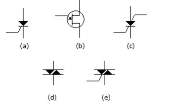
Identify the symbol for an SCS.
a
b
c
d
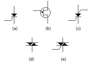
Identify the triac from the given figures.
a
e
d
b
Your boss has asked you to recommend a thyristor that will enable you to turn it on with a pulse and also turn it off with a pulse. Which of the following should you recommend?
an SCS
an SCR
a PUT
a triac
You have a light-dimmer circuit using an SCR. In testing the circuit, you find that IG = 0 mA and the light is still on. You conclude that the trouble might be one of the following:
the gate circuit is shorted.
the SCR is open.
this is normal; nothing is wrong.
the switch is faulty
An SCR acts to control the speed of an electric motor by ____ the ____ of the pulse delivered to the motor.
decreasing, gate width
varying, width
none of these
increasing, amplitude
What is the voltage drop across Schottky diodes?
0.7 V to 0.8 V
0.8 V to 1.0 V
1.0 V to 1.5 V
0 V to 0.2 V
In which region is the operating point stable in tunnel diodes?
Neither negative- nor positive-resistance
Positive-resistance
Both negative- and positive-resistance
Negative-resistance
What is the maximum temperature limit for liquid-crystal displays (LCDs)?
10ºC
30ºC
100ºC
60ºC
What is the limit of peak current IP in tunnel diodes?
A few microamperes to several hundred microamperes
A few microamperes to several hundred amperes
A few microamperes to several milliamperes
A few microamperes to several amperes
What is the response time of LCDs?
50 ms
100 ms to 300 ms
Less than 100 ns
400 ms
What is the typical level of change in resistance per degree change in temperature?
10% to 25%
1% to 2%
3% to 5%
7% to 10%
What is the maximum peak voltage for tunnel diodes?
50 mV
250 mV
600 mV
100 mV
What is the power density received from the sun at sea level?
500 mW/cm2
1 W/cm2
100 mW/cm2
10 mW/cm2
What is the resistance of thermistors at boiling temperature (100ºC)?
1Ω
100Ω
1 kΩ
5 kΩ
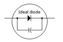
This is an approximate equivalent circuit for the ________ diode.
Schottky
PIN
varicap
tunnel
What is the ratio IP / IV for gallium arsenide?
5:1
20:1
1:1
10:1
What is the response time of cadmium sulfide (CdS) in photoconductive cells?
25 ms
100 ms
50 ms
10 ms
A 339 IC is an example of a fourteen-pin DIP that can be made to function as a ________.
D to A converter
comparator
555 timer
ladder network
What is the minimum number of conversions per second of a clock rate of 1 MHz operating a 10-stage counter in an ADC?
769
1000
697
976
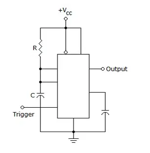
Which application best describes this 555 timer circuit?
Astable multivibrator
Free-running multivibrator
Bistable multivibrator
Monostable multivibrator
What is the first phase of the dual-slope method of conversion?
Connecting the analog voltage to the integrator for a fixed time
All of the above
Setting the counter to zero
Connecting the integrator to a reference voltage
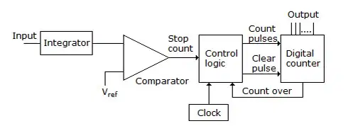
This figure is a block diagram of a(n) ________.
ADC
comparator
DAC
555 timer
What is the function of a ladder network?
Changing an analog signal to a digital signal
None of the above
Changing a linear signal to a digital signal
Changing a digital signal to an analog signal
At which of the following period(s) is the counter advanced (incremented) in dual-slope conversion?
None of the above
During the charging of the capacitor of the integrator
During the discharging of the capacitor of the integrator
During both the charging and discharging of the capacitor of the integrator
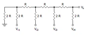
This circuit is an example of a ________.
555 timer
ladder network
D to A converter
comparator
When is the counter set to zero in the dual-slope method of conversion?
During the discharging of the capacitor
Prior to the charging of the capacitor of the integrator
At the end of the charging of the capacitor
While the capacitor is being charged
How many Vcc connections does the 565 PLL use?
2
1
3
0
The timing components for a PLL are 15 k and 220 pF. Calculate the free running frequency.
90.91 kHz
181.8 kHz
156.1 kHz
136.36 kHz
Which of the following best describes the output of a 566 voltage controlled oscillator?
Square-wave
Both square- and triangular-wave
None of the above
Triangular-wave