
 Worksheets
Photolithography and Etching Processes
Total questions: 12
Worksheet time: 6mins
What is photolithography?
A process to produce a 3D pattern on the surface of the wafer using a light sensitive photoresist material and controlled exposure to light.
A method for etching patterns on silicon wafers.
A technique for polishing semiconductor surfaces.
What are the major steps in the photolithography process?
Spin coat, Soft bake, Alignment and Exposure, Post-exposure bake, Develop, Hard bake, Inspect.
Implant, Diffusion, Test/Sort, Etch, Polish.
Coating, Etching, Ion implantation.
What are the two basic types of processes in lithography?
Negative resist and Positive resist.
Wet etch and Dry etch.
Oxidation and Doping.
What is the purpose of photolithography in wafer fabrication?
To transfer the mask pattern to the photoresist on the top layer of the wafer surface.
To remove unwanted materials from the wafer.
To polish the wafer surface.
What is etching?
A process of selectively removing the unwanted material from the surface of the wafer.
A method for applying photoresist to wafers.
A technique for aligning photomasks.
What are the two types of etching methods?
Wet etch and Dry etch.
Positive resist and Negative resist.
Photolithography and Ion implantation.
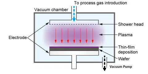
What are the types of etching methods mentioned in the figure?
Wet etch which uses chemicals
Dry etch which uses active ionized gases/plasma
What is the disadvantage of wet etching?
It can cause undercutting
It is more expensive than dry etching
What is the purpose of endpoint detection in dry etching?
To monitor the etching process
To increase the etch rate
What is the main disadvantage of dry etching?
Poor selectivity to the underlying layer
It is more expensive than wet etching
What is CMP in the context of planarization?
Chemical Mechanical Planarization
Chemical Metal Planarization
What does CMP provide in terms of wafer surface?
Best flatness
Best roughness

