
 Worksheets
PN Junctions and Semiconductor Concepts
Total questions: 13
Worksheet time: 10mins
In a p-type semiconductor, what are the majority charge carriers?
Electrons
Holes
Protons
Neutrons
What is the primary characteristic of the depletion region in an unbiased PN junction?
It contains a high concentration of free charge carriers.
It is devoid of free charge carriers but contains immobile ions.
It is a region of high electrical conductivity.
It is formed only under external biasing conditions.
What is the approximate built-in potential barrier for a silicon PN junction at room temperature?
0.3 V
0.7 V
1.1 V
1.5 V
In a forward-biased PN junction, what happens to the width of the depletion region?
It increases.
It decreases.
It remains unchanged.
It fluctuates randomly.
What is the primary mechanism for current flow in a forward-biased PN junction when the applied voltage exceeds the barrier potential?
Increased resistance in the depletion region.
Movement of minority carriers across the junction.
Diffusion of majority carriers across the now negligible resistance of the depletion region.
Generation of new electron-hole pairs due to high electric field.
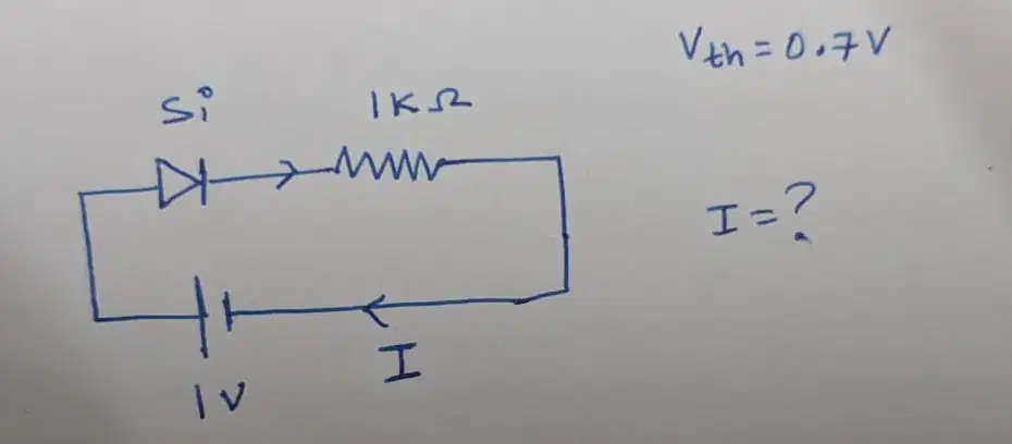
What is the current flowing in the circuit ? Assume diode drop = Vth for silicon diode.
0.66 mA
0.3 mA
1 mA
0.1 mA
A P-type semiconductor is overall:
Positively charged
Negatively charged
Electrically neutral
Depends on amount of doping
In a p-type semiconductor, which of the following is correct?
Fixed positive ions
Fixed negative ions
Mobile negative electrons
None of the above
In a silicon transistor in active region, if base current = 20 μA and current gain β = 100, then the collector current is:
0.2mA
2mA
20mA
200mA
In the active region of a BJT, which statement is correct?
Base-Emitter junction reverse biased, Base-Collector forward biased
Both junctions reverse biased
Base-Emitter forward biased, Base-Collector reverse biased
Both junctions forward biased
A transistor is said to be in saturation when:
IC=βIB
VCE is maximum
VCE is very small (close to 0.2 V for silicon)
Base current is zero
In a common emitter amplifier, the phase difference between input and output voltage is:
0°
90°
180°
360°
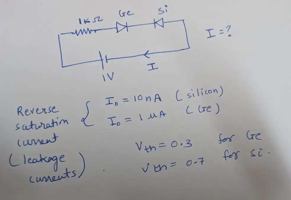
What is the current I flowing through the circuit?
1 nA
10 nA
1uA
10 uA

