
Font size
 Worksheets
Transistor Biasing Methods Introduction and Base Bias Theory
Total questions: 13
Worksheet time: 7mins
In designing for the theoretical ideal operating point (Q-point) on the load line for maximum undistorted signal swing, which approximate conditions are targeted?
IC ≈ IC(sat), VCE ≈ 0 V
IC ≈ 0, VCE ≈ VCC
IC ≈ IC(sat)/2, VCE ≈ VCC/2
IC ≈ β IB/2, VCE ≈ VBB/2
For a base bias (fixed bias) BJT with emitter grounded, which equation correctly gives the base current IB in terms of supply and resistor values?
IB = (VCC − VCE)/RC
IB = (VBB − VBE)/RB
IB = β (VBB − VBE)
IB = (VCC − IC RC)/RB
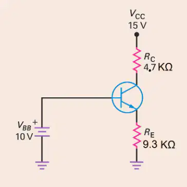
For the emitter-bias circuit shown (with VCC, RC, and RE indicated), which equation correctly gives the collector–emitter voltage VCE in terms of supply and current variables?
VCE = VCC + ICRC + IERE
VCE = VCC − ICRC − IERE
VCE = VBB − IBRB − VBE
VCE = VBB + ICRC − IERE
Which biasing method offers good β-stability because the emitter current is largely set by RE, making it weakly affected by β via VBE?
Base bias
Emitter bias
None of the above
Collector feedback bias
What is the primary purpose of a coupling capacitor in an amplifier circuit?
To increase the DC bias voltage at the input
To connect the AC signal while blocking DC to avoid disturbing the Q-point
To reduce the amplifier’s input resistance
To stabilize β variations with temperature
Using the 10:1 rule for a coupling capacitor, if the lowest frequency of operation is 20 Hz and the resistance seen by the capacitor is 2 kΩ, what is the approximate capacitance needed for good coupling? Use Xc = 1/(2πfC) and set Xc = 0.1R at the lowest frequency.
3.98 µF
39.8 µF
0.398 µF
398 µF
19.9 µF
In the collector voltage waveform diagram labeled VCE versus time, the sinusoid is centered about a DC level marked +V. What does +V indicate in this context?
The peak output voltage
The DC collector voltage (quiescent level)
The emitter bias voltage
The RMS output voltage
Which pairing correctly matches each waveform to the transistor quantity it represents?
(a) collector current, (b) base current, (c) emitter voltage
(a) base current, (b) collector current, (c) collector voltage
(a) emitter current, (b) base voltage, (c) collector current
(a) base voltage, (b) collector voltage, (c) base current
In the Voltage Divider Bias amplifier diagram, which component is explicitly labeled with a value of 5 kΩ?
Emitter resistor R_E
Collector resistor R_C
Input coupling capacitor
Load resistor R_L
Which statement best characterizes the relationship between the DC and AC components in the provided waveforms and amplifier diagram?
DC components determine small-signal gain, while AC components set the bias point.
AC components establish the operating point; DC components are removed by coupling capacitors.
DC components set the operating (quiescent) point; AC components represent signal variations about that point.
Neither DC nor AC components affect amplifier operation.
In a common-emitter amplifier configuration, what is the effect of increasing the collector resistor RC on the voltage gain of the amplifier?
The voltage gain decreases
The voltage gain increases
The voltage gain remains constant
The voltage gain becomes zero
What is the role of the bypass capacitor in an emitter follower configuration?
To reduce the output impedance
To allow AC signals to pass while blocking DC
To stabilize the DC operating point
To increase the input impedance
In a transistor amplifier, what does the term 'quiescent point' (Q-point) refer to?
The point of minimum distortion in the output signal
The point where the transistor is turned off
The DC operating point of the transistor
The point of maximum output power

