
Font size
 Worksheets
ASIC Design Flow Procedure using Cadence Tool Suite
Total questions: 18
Worksheet time: 9mins
Which of the following is the correct first step to create a workspace for an ASIC design project using the Cadence Tool Suite?
Make a right click on the Desktop and select the option 'New Folder'.
Open the Cadence Tool Suite and select 'Create Project'.
Type 'cshell' in the terminal to create a workspace.
Download the workspace template from the internet.
In the ASIC design flow procedure, which technology nodes are available for synthesis, and what is the name of the synthesis tool used?
The available technology nodes are 180nm, 90nm, and 45nm, and the synthesis tool used is 'Genus'.
The available technology nodes are 130nm, 65nm, and 28nm, and the synthesis tool used is 'Virtuoso'.
The available technology nodes are 180nm, 90nm, and 65nm, and the synthesis tool used is 'Spectre'.
The available technology nodes are 45nm, 28nm, and 14nm, and the synthesis tool used is 'Genus'.
What does Moore's law state about the scale of integrated circuits (ICs)?
The scale of ICs has doubled every 18 months.
The scale of ICs has halved every 18 months due to technological limitations.
The scale of ICs remains constant over time.
The scale of ICs changes randomly every year.
Select all correct statements about feature size in integrated circuits (ICs).
Feature size refers to the size of transistors and interconnecting wires in ICs.
Decreasing feature size has resulted in increased operating frequencies and clock speeds.
Feature size has increased from tens of microns to hundreds of microns over time.
Current submicron technologies are based on feature sizes of less than 100 nanometers.

Refer to the diagram showing the VLSI development process. Which stage comes immediately after 'Fabrication'?
Wafer Test
Design Verification
Packaging
Final Testing

Refer to the diagram showing the design hierarchy in VLSI. Which level comes directly after the Behavioral (Architecture) Level in the design process?
Register-Transfer Level
Logical (Gate) Level
Physical (Transistor) Level
What is the formula for calculating the yield of a manufacturing process in VLSI testing?
Yield = Number of acceptable parts / Total number of parts fabricated
Yield = Number of faulty parts passing final test / Total number of parts passing final test
Yield = Number of parts passing initial test / Total number of parts fabricated
What does the mean time between failures (MTBF) represent in reliability engineering?
The expected time between two consecutive failures of a system
The total time a system operates before its first failure, including repair time
The average time required to repair a system after a failure
The probability that a system will operate normally until a given time
What is the formula for fault coverage in the context of VLSI circuit testing?
Fault coverage = Number of detected faults / Total number of faults
Fault coverage = Total number of faults / Number of detected faults
Fault coverage = Number of detected faults × Total number of faults
Fault coverage = Number of detected faults + Total number of faults
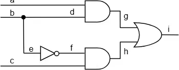
Refer to the example circuit diagram. If a stuck-at-0 fault occurs on fanout branch line d, how does this affect the output y?
The output y will behave differently than if a stuck-at-0 fault occurs on fanout branch line e.
The output y will be the same as if a stuck-at-0 fault occurs on fanout branch line e.
The output y will always be logic 0 regardless of the input.
The output y will always be logic 1 regardless of the input.
Which formula is used to calculate the number of collapsed faults in a combinational circuit constructed from elementary logic gates?
Number of collapsed faults = 2 × (number of POs + number of fanout stems) + total number of gate (including inverter) inputs − total number of inverters.
Number of collapsed faults = (number of POs × number of fanout stems) − total number of gate inputs + total number of inverters.
Number of collapsed faults = number of gate inputs × number of inverters × number of fanout stems.
Number of collapsed faults = (number of POs + number of gate inputs) ÷ total number of inverters.
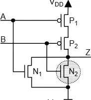
Refer to the diagram of the two-input CMOS NOR gate. Which type of transistor fault creates a conducting path between VDD and VSS, resulting in a voltage divider at the output node Z?
Stuck-open fault, which requires a sequence of two vectors for detection.
Stuck-short fault, which may be detected by monitoring the steady-state power supply current (IDDQ testing).
Stuck-at fault, which is detected by a single test vector.
Latch fault, which causes the output to retain its previous state.
What is the formula for calculating the number of collapsed transistor faults in a circuit, where T is the total number of transistors, Ts is the total number of transistors in series, Gs is the total number of groups of transistors in series, Tp is the total number of transistors in parallel, and Gp is the total number of groups of transistors in parallel?
Number of collapsed faults = 2 × T − Ts + Gs − Tp + Gp
Number of collapsed faults = T × Ts + Gs × Tp + Gp
Number of collapsed faults = T + Ts + Gs + Tp + Gp
Number of collapsed faults = 2 × T + Ts − Gs + Tp − Gp

Refer to Figure 1.9, which illustrates various bridging fault models in VLSI circuits, including wired-AND, wired-OR, and dominant bridging fault models. Which statement best describes the difference between the wired-AND and dominant-AND bridging fault models?
In the wired-AND model, the signal net takes a logic 0 if either shorted line is sourcing a logic 0, while in the dominant-AND model, one driver dominates the logic value of the shorted nets only for a given logic value.
In the wired-AND model, the signal net takes a logic 1 if either shorted line is sourcing a logic 1, while in the dominant-AND model, both drivers must source a logic 1 for the net to be logic 1.
The wired-AND model is used only for resistive shorts, while the dominant-AND model is used for open faults.
The dominant-AND model always produces the same output as the wired-AND model regardless of the input values.
Which of the following best describes a path-delay fault in a logic circuit?
A fault that considers the cumulative propagation delay along a signal path through the circuit.
A fault that only considers the delay at a single gate in the circuit.
A fault that is caused by a short circuit between two signal lines.
A fault that occurs when the output of a gate is stuck at a constant value.
What is the primary function of the slow.lib library in Cadence tools?
To represent the worst-case timing scenario and ensure the chip meets performance requirements under unfavorable operating conditions.
To speed up the design process by minimizing propagation delay in logic gates and wires.
To optimize the chip for the fastest possible operating conditions only.
To check for syntax errors in hardware description language files.
Which statement best describes the effect of setting the syn_map_effort attribute to 'high' in a synthesis tool?
It applies more aggressive and time-consuming optimization algorithms to achieve the best possible Quality of Results (QoR), potentially reducing area further or improving timing sign-off results.
It uses fewer algorithms and less runtime, suitable for quick check runs where speed is more important than final Power, Performance, and Area (PPA) optimization.
It provides a balance between runtime, QoR, and optimization algorithms, employing a standard set of algorithms to meet timing requirements, minimize area, and optimize power consumption.
What does a negative slack value in a timing report indicate?
It indicates a timing violation in the design.
It means the design meets all timing requirements with margin.
It shows the design has no setup time violations.
It represents the total delay from the clock source.

