
 Worksheets
Introduction to Basic Electronics
Total questions: 20
Worksheet time: 11mins

What is the voltage across the terminals A & B ? Assume both the sources and connecting wires are ideal.
5 V
10 V
15 V
10/3 V
None of the above
Series connected resistance of 5 Ω and 10 Ω is equal to
10 Ω
50 Ω
15 Ω
20 Ω
Graphite is a :
conductor
insulator
semiconductor
none of these
Which of the following doesn’t have forbidden energy gap between valence band and conductor band ?
conductor
insulator
semiconductor
None of the above
The battery connections required to forward bias a pn junction are ……..
+ve terminal to p and -ve terminal to n
-ve terminal to p and +ve terminal to n
-ve terminal to p and -ve terminal to n
none of the above
A semiconductor in its purest form is called.......
Extrinsic semiconductor
Superconductor
Intrinsic semiconductor
Insulator
For a silicon P-N junction, the barrier potential is about
0.7 V
0.8 V
0.9 V
1.0 V
In series, if one bulb goes out, others will
stay on
also turn off
blow up
heat up
Which of these colors is NOT used in the resistor value color code?
white
black
violet
pink
Which one is a 3 terminal device?
Varactor diode
LASER diode
Transistor
LED
Which one is NPN transistor?


The insulating layer in MOSFET is
SiO2
Ge
Si
Mica
LAN stands for:
Least Access Network
Least Area Network
Local Area Network
Local Access Network
Noise is ....... signal
Predictable
Random
Necessary
Both b & c
The communication medium causes the signal to be
amplified
attenuated
modulated
detected
The process of superimpossing a baseband signal over a high frequency carrier signal is
demodulation
modulation
detection
multiplexing

The truth table shows possible output for ____ gate.
NOT
AND
OR
NAND
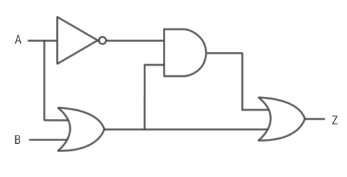
What is the output Z of this logic circuit, if A=1 and B=1?
0
1
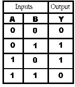
The given truth table belongs to which logic gate?
Which device is commonly used in electronic circuits to stores electric charge?
Inductor
Potentiometer
Capacitor
Diodes

