
 Worksheets
Semiconductor-Diodes-Voltage-Dividers
Total questions: 136
Worksheet time: 4hrs 40mins
Intrinsic semiconductor material is characterized by a valence shell of how many electrons?
A.1
B.2
C.4
D.6
One eV is equal to ________ J.
A. 6.02 × 10^23
B. 1.6 × 10^-19
C. 6.25 × 10^18
D. 1.66 × 10^-24
The diode ________.
A. is the simplest of semiconductor devices
B. has characteristics that closely match those of a simple switch
C. is a two-terminal device
D. All of the above
It is not uncommon for a germanium diode with an Is in the order of 1-2 uA at 25°C to have leakage current of 0.1 mA at a temperature of 100°C.
A. True
B. False
What does a high resistance reading in both forward- and reverse-bias directions indicate?
A. A good diode
B. An open diode
C. A shorted diode
D. A defective ohmmeter
Which capacitance dominates in the reverse-bias region?
A. depletion
B. conversion
C. Diffusion
D. None of the above
Which capacitance dominates in the forward-bias region?
A. depletion
B. conversion
C. Diffusion
D. None of the above
What is the state of an ideal diode in the region of nonconduction?
A. An open circuit
B. A short circuit
C. Unpredictable
D. Undefined
How many orbiting electrons does the germanium atom have?
A. 4
B. 14
C. 32
D. 41
How many terminals does a diode have?
A. 1
B. 2
C. 3
D. 4
What unit is used to represent the level of a diode forward current IF?
A. pA
B. nA
C. uA
D. mA
The diffused impurities with ________ valence electrons are called donor atoms.
A. 4
B. 3
C. 5
D. 0
In which of the following color(s) is (are) LEDs presently available?
A. Yellow
B. White
C. Orange
D. All of the above
Determining rd to a high degree of accuracy from a characteristic curve is very accurate.
A. True
B. False
What is the range of the operating voltage level for LEDs?
A. 5-12 mV
B. 1.7-3.3 V
C. 5-12 V
D. 20-25 V
At what kind of operating frequency diffusion or transition is a capacitor represented in parallel with the ideal diode?
A. Low frequency
B. Moderate frequency
C. Mid frequency
D. Very high frequency
Which of the following devices can check the condition of a semiconductor diode?
A. Digital display meter (DDM)
B. Multimeter
C. Curve tracer
D. All of the above
Ionization within a P-N junction causes a layer on each side of the barrier called the:
A. junction
B. depletion region
C. barrier voltage
D. forward voltage
What is the most significant development in electronics since World War II?
A. the development of color TV
B. the development of the diode
C. the development of the transistor
D. the development of the TRIAC
What causes the depletion region?
A. doping
B. diffusion
C. barrier potential
D. ions
What is an energy gap?
A. the space between two orbital shells
B. the energy equal to the energy acquired by an electron passing a 1 V electric field
C. the energy band in which electrons can move freely
D. an energy level at which an electron can exist
Silicon atoms combine into an orderly pattern called a:
A. covalent bond
B. crystal
C. semiconductor
D. valence orbit
In "n" type material, majority carriers would be:
A. holes
B. dopants
C. slower
D. electrons
Elements with 1, 2, or 3 valence electrons usually make excellent:
A. conductors
B. semiconductors
C. insulators
D. neutral
A commonly used pentavalent material is:
A. arsenic
B. boron
C. gallium
D. neon
Which material may also be considered a semiconductor element?
A. carbon
B. ceramic
C. mica
D. argon
In "p" type material, minority carriers would be:
A. holes
B. dopants
C. slower
D. electrons
What can a semiconductor sense?
A. magnetism
B. temperature
C. pressure
D. all of the above
When an electron jumps from the valence shell to the conduction band, it leaves a gap. What is this gap called?
A. energy gap
B. hole
C. electron-hole pair
D. recombination
Forward bias of a silicon P-N junction will produce a barrier voltage of approximately how many volts?
A. 0.2
B. 0.3
C. 0.7
D. 0.8
Which semiconductor material is made from coal ash?
A. germanium
B. silicon
C. tin
D. carbon
When and who discovered that more than one transistor could be constructed on a single piece of semiconductor material:
A. 1949, William Schockley
B. 1955, Walter Bratten
C. 1959, Robert Noyce
D. 1960, John Bardeen
When is a P-N junction formed?
A. in a depletion region
B. in a large reverse biased region
C. the point at which two opposite doped materials come together
D. whenever there is a forward voltage drop
A P-N junction mimics a closed switch when it:
A. has a low junction resistance
B. is reverse biased
C. cannot overcome its barrier voltage
D. has a wide depletion region
Solid state devices were first manufactured during:
A. World War 2
B. 1904
C. 1907
D. 1960
Electron pair bonding occurs when atoms:
A. lack electrons
B. share holes
C. lack holes
D. share electrons
How many valence electrons are in every semiconductor material?
A. 1
B. 2
C. 3
D. 4
What is a type of doping material?
A. extrinsic semiconductor material
B. pentavalent material
C. n-type semiconductor
D. majority carriers
Minority carriers are many times activated by:
A. heat
B. pressure
C. dopants
D. forward bias

What is the voltage across R1 if the P-N junction is made of silicon?
A. 12 V
B. 11.7 V
C. 11.3 V
D. 0 V
If conductance increases as temperature increases, this is known as a:
A. positive temperature coefficient
B. negative current flow
C. negative temperature coefficient
D. positive resistance
Which of the following cannot actually move?
A. majority carriers
B. ions
C. holes
D. free electrons
What electrical characteristic of intrinsic semiconductor material is controlled by the addition of impurities?
A. conductivity
B. resistance
C. power
D. all of the above
The forward voltage drop for a germanium transistor is 0.7 V and for a silicon transistor is 0.3 V.
A. True
B. False
When a depletion region of a transistor is large the barrier voltage is also large.
A. True
B. False
The first integrated circuit was invented in 1959.
A. True
B. False
A covalent bond is when atoms lose valence shell electrons.
A. True
B. False
When a voltage is placed across a semiconductor, free electrons move toward the negative voltage.
A. True
B. False
The first transistor was invented in 1938.
A. True
B. False
Germanium is the most widely used semiconductor material because of its stability at high temperatures.
A. True
B. False
The natural elements carbon, germanium, and silicon are semiconductors.
A. True
B. False
The P-N junction is a barrier to electron flow.
A. True
B. False
The number of electrons in the outer shell of carbon, germanium, and silicon is 5.
A. True
B. False
The n-type semiconductor material is doped by adding material with electron holes.
A. True
B. False
Reverse bias is a condition that essentially ___________ current through the diode.
A. allows
B. prevents
C. increases
D. blocks
Atoms that normally have three electrons in their outer shell are called __________________ atoms.
A. trivalent
B. pentavalent
C. tetravalent
D. charged
Assume the valence electron is removed from a copper atom. The net charge of the atom becomes:
A. 0
B. +1
C. -1
D. +4
At absolute 0 temperature, an intrinsic semiconductor has:
A. a few electrons
B. many holes
C. many electrons
D. no holes or free electrons
As the forward current through a silicon diode increases, the voltage across the diode:
A. increases to a 0.7 V maximum
B. decreases
C. is relatively constant
D. decreases and then increases
When a pure semiconductor is heated, its resistance.
A. decreases
B. increases
C. remains the same
D. can’t say
A semiconductor has _____ temperature coefficient of resistance.
A. Positive
B. Zero
C. Negative
D. None of the above
The most commonly used semiconductor is
A. Germanium
B. Silicon
C. Carbon
D. Copper
When a pentavalent impurity is added to a pure semiconductor, it becomes
A. an insulator
B. an intrinsic semiconductor
C. p-type semiconductor
D. n-type semiconductor
Addition of pentavalent impurity to a semiconductor creates many
A. free electrons
B. holes
C. valence electrons
D. bound electrons
An n-type semiconductor is
A. positively charged
B. negatively charged
C. electrically neutral
D. none of the above
When a trivalent impurity is added to a pure semiconductor it becomes
A. an insulator
B. an intrinsic semiconductor
C. p-type semiconductor
D. n-type semiconductor
As the doping to a pure semiconductor increases, the bulk resistance of the semiconductor.
A. remains the same
B. increases
C. decreases
D. none of the above
In the depletion region of a pn junction, there is shortage of
A. acceptor ions
B. holes and electrons
C. donor ions
D. none of the above
In a PN junction with no external voltage, the electric field between acceptor and donor ions is called a
A. peak
B. barrier
C. threshold
D. path
In a PN junction the potential barrier is due to the charges on either side of the junction, these charges are
A. majority carriers
B. minority carriers
C. both a and b
D. fixed donor and acceptor ions
The capacitance of a reverse biased pn junction
A. increases as reverse bias is increased
B. decreases as reverse bias is decreased
C. increases as reverse bias is decreased
D. is significantly low
For a PN junction, the current in reverse bias may be
A. few milliamperes
B. between 0.2A and 15A
C. few amperes
D. few micro or nano amperes
When a PN junction is reverse-biased
A. Majority carriers tend to concentrate towards the junction
B. the barrier tends to break down
C. majority carriers tend to move away from the junction
D. none of the above
During reverse bias, a small current develops known as a
A. forward current
B. passive current
C. reverse saturation current
D. active current
Determine the bulk resistance of a diode for a forward voltage of 0.93 V at 1 ampere. (Assume Si diode is used)
A. 0.23 ohm
B. 0.53 ohm
C. 0.73 ohm
D. 0.93 ohm
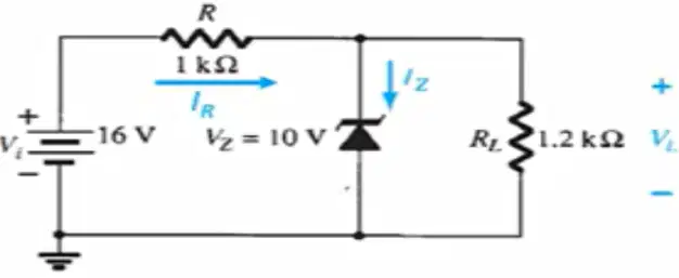
Solve for P_Z in the circuit shown.
a. 6.35mW
b. 2.2mW
c. 8.1mW
d. 0W

Solve for P_Z in the circuit shown if R_L=3 kΩ.
a. 26.7mW
b. 18.2mW
c. 12.5mW
d. 0W
Which of the following are true?
1) point contact diode has a metal whisker to make pressure contact during its operation
2) it has high voltage rating
3) its V-I characteristics are constant
4) it has low breakdown voltage
A. 1 and 2
B. 3 only
C. 1 and 4
D. 2 only
Schottky diodes are also known as
A) minority carrier diode
B) hot carrier diode
C) majority carrier diode
D) electrode carrier diode
Diode used primarily in high frequency devices and fast switching applications is called
A) current regulator diode
B) Schottky diode
C) PIN diode
D) Zener diode
The capacitance of varactor varies
A) inversely with reverse voltage
B) very slightly independent with reverse voltage
C) independent of reverse voltage
D) directly with reverse voltage
Varactor diodes are used in FM receivers to obtain
A) automatic frequency control
B) automatic noise control
C) automatic volume control
D) automatic gain control
The tunneling involves
A) acceleration of electrons in p side
B) movement of electrons from n side conduction band to p side valence band
C) charge distribution management in both bands
D) positive slope characteristics of diode
The depletion layer of tunnel diode is very small because
A) its abrupt and has high dopants
B) uses positive conductance property
C) its used for high frequency ranges
D) tunneling effect
Light which has one single wavelength is called
A) coherent
B) incoherent
C) neutral
D) emitter
Laser diode has
A) coherent light
B) incoherent light
C) radio light
D) microwave light
PIN diode consist of
A) 2 operating regions
B) 3 operating regions
C) 4 operating regions
D) 5 operating regions
In fiber optic systems, types of PIN diodes are used as
A) photodetectors
B) photoresistors
C) tuner
D) transmitter
Which of the following materials can be used to produce infrared LED?
A) Si
B) GaAs
C) CdS
D) PbS
Photodiode is used in the detection of
A) visible light
B) invisible light
C) no light
D) both visible and invisible light
In photodiode, when there is no incident light, the reverse current is almost negligible and is called
A) Zener current
B) dark current
C) photo current
D) PIN current
One that clips the positive part of the voltage is known as
A) current regulator
B) clipper
C) multimeter
D) voltage regulator
Which of the following value is varied in a clamper circuit?
a. AC
b. DC
c. Alternative Current
d. Both a and c
Clamper circuits are majorly used in _____ applications?
a. FM transmitters
b. Analog television
c. Removes distortion
d. All the above
Which of the following component in clamper circuit shifts wave?
a. Diode
b. Resistor
c. Capacitor
d. All the above

Identify the circuit displayed below?
a. Series Negative Clipper
b. Series Positive Clipper
c. Series Negative Clamper
d. Series Positive Clamper
Addition of another diode capacitor section to half wave voltage tripler creates a
A) voltage doubler
B) voltage quadrupler
C) voltage generator
D) voltage regulator
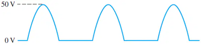
What is the average value of the half-wave rectified voltage in the figure?
a. 25.57V
b. 15.92V
c. 43.23V
d. 37.89V
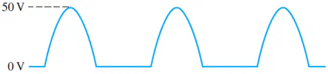
Determine the PIV of the diode in the given figure.
a. 85V
b. 159V
c. 70V
d. 124V
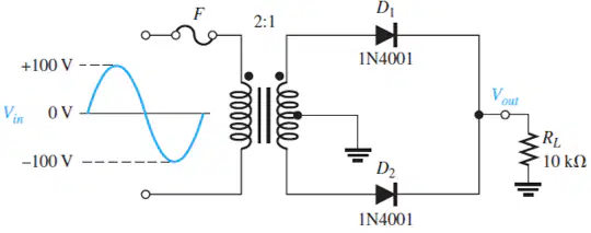
Determine the voltage across R_L when a 100 V peak sine wave is applied to the primary winding in the figure below.
a. 13.5V
b. 45.8V
c. 75.2V
d. 24.3V
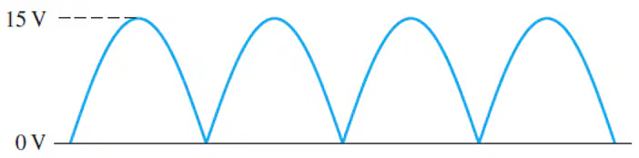
Find the average value of the full-wave rectified voltage in figure?
a. 10.93V
b. 12.84V
c. 9.55V
d. 8.78V

Determine the peak output voltage for the bridge rectifier in the given figure. The transformer is specified to have a 12 V rms secondary voltage for the standard 120 V across the primary.
a. 28.12V
b. 15.57V
c. 10.64V
d. 8.78V
Calculate the dc voltage across a 1-kΩ load for an RC filter section (R=120Ω, C=10uF). The dc voltage across the initial filter capacitor is V_DC 60V.
a. 53.6 V
b. 26.34 V
c. 63.86 V
d. 17.32 V
Calculate the output voltage of an LM317 voltage regulator if R_1=240Ω and R_2=2.4kΩ.
a. 14 V
b. 21 V
c. 27 V
d. 30 V
A certain 7805 regulator has a measured no-load output voltage of 5.18 V and a full load output of 5.15 V. What is the load regulation expressed as a percentage?
a. 0.29 %
b. 0.07 %
c. 0.58 %
d. 0.50 %
What is the resistor value of an ideal diode in the region of conduction?
A) 0
B) 5k
C) Undefined
D)Infinity
What is the state of an ideal diode in the region of non conduction?
A) An open circuit
B) A short circuit
C) Unpredictable
D) Undefined
The ideal diode is a(n) ______ circuit in the region of non conduction.
A) Open
B) Short
Which of the following is an atom composed of?
A) Electrons
B) Protons
C) Neutrons
D) All of the above
How many valence electrons does a silicon atom have?
A) 1
B) 2
C) 3
D) 4
How many orbiting electrons does a Germanium atom have?
A) 4
B) 14
C) 32
D) 41
A 12V AC to DC power supply has a transformer with turns ratio of 4:1. What is the peak secondary voltage if 115V peak is applied to the primary winding?
a. 28.75V
b. 32.56V
c. 23.91V
d. 41.53V
What is the peak secondary voltage on a transformer having a secondary to primary turns ratio of 1:14?
a. 15.12V
b. 22.22V
c. 53.17V
d. 86.63V
A 200 KVA-rated transformer has a full-load copper loss of 1.5 KW and an iron loss of 1 KW. Determine the transformer efficiency at full load and 0.85 power factor.
a. 85.9%
b. 79.1%
c. 98.6%
d. 90.2%
A full-wave rectifier with peak rectified voltage of 30V feeds a 100uF filter capacitor connected to a load drawing 50mA. Calculate the ripple factor.
a. 0.01
b. 0.02
c. 0.03
d. 0.04
What is/are the purposes(s) of RL?
A. It limits the amount of current flow in the circuit
B. It develops the output signal
C. Both A and B above
D. It maintains the proper bias on the diode
If the input frequency to a half-wave rectifier is 120 hertz, what is the output frequency of the rectified dc?
A. 30 pps
B. 60 pps
C. 120 pps
D. 240 pps
One of the prime dangers to the semiconductor diode is heat. Excessive current generated by heat which eventually destroys a diode is called
A. junction overload
B. thermal runaway
C. thermoplastic action
D. thermionic emission
Which of the following elements is the most frequently used for doping pure Ge or Si?
A) Boron
B) Gallium
C) Indium
D) All of the above
The diffused impurities with _______ valence electrons are called donor atoms.
A) 4
B) 3
C) 5
D) 0
In what state is a silicon diode if the voltage drop it is about 0.7V?
A) No bias
B) Forward Bias
C) Reverse bias
D) Zener region
Which of the following is true?
Si diodes have higher PIV and narrower temperature ranges than Ge diodes.
Si diodes have higher PIV and wider temperature ranges than Ge diodes.
Si diodes have lower PIV and narrower temperature ranges than Ge diodes.
Si diodes have lower PIV and wider temperature ranges than Ge diodes.
It is not uncommon for a germanium diode with an Is in the order of 1-2A at 25 degrees Celsius to have a leakage current of 0.1 mA at a temperature of 100 degrees Celsius
a) True
B) False
Calculate the static resistance RD of a diode having ID = 30mA and VD = 0.75V.
A) 25
B) 40
C) 0.04
D) 0.025
Calculate ID if RD = 30 Ohms and VD = 0.84V
A) 28 mA
B) 0.028mA
C) 2.8mA
D) 280A
Refer to the Figure 1.27, Calculate the dynamic resistance RD of a diode having ID = 27.5mA.
A) 0
B) 2
C) 5
D) 26
Determining rd to a high degree of accuracy from a characteristic curve is very accurate.
A) True
B) False
The _______ diode model is employed most frequently in the analysis of electronic systems.
A) ideal device
B) simplified
C) piecewise-linear
D) none of the above
Calculate the power dissipation of a diode having ID =40mA.
A) 28mW
B) 28W
C) 280mW
D) Undefined
What is the value of the transition capacitance for a silicon diode when VD=0?
A) 1pF
B) 3pF
C) 5pF
D) 10pF
Calculate the temperature coefficient in %/ degrees celsius of a 10-V nominal Zener diode at 25 degrees celsius if the nominal voltage is 10.2 V at 100 degrees celsius.
A) 0.0238
B) 0.0251
C) 0.0267
D) 0.0321
What is the maximum power rating for LEDs?
A) 150mW
B) 500mW
C) 1W
D) 10W
In which of the following is the light intensity measured?
A) Candela
B) Efficacy
C) Flux
D) Illumination
The term ______ is often used when comparing the resistance level of materials.
A) permittivity
B) inductivity
C) conductivity
D) resistivity
In the atomic lattice the ____ and ___ form the nucleus.
A) electrons, neutrons
B) electrons, protons
C) neutrons, protons
D) none of the above
An increase in the temperature of a semiconductor can result in a _____ in the number of free electrons in the material.
A) substantial increase
B) substantial decrease
C) slight decrease
D) no change

