
 Worksheets
Semiconductors
Total questions: 36
Worksheet time: 18mins
Which among these is the fundamental characteristic of a p type semiconductor
Electrons are the majority charge carriers
Has a tendency to gain an electron
Has a tendency to donate an electron
Easy to conduct electricity
Who contribute to the current in a semiconductor
electrons only
holes only
negative ions
both electrons and holes
____________ are the charge carriers in N- type semiconductors.
electrons
protons
holes
neutrons
P, Sb, As doped with pure Si are the examples of
P-type semiconductor
Penta valent impurities
Intrinsic semiconductors
N-type semiconductors
For intrinsic semiconductor, the number of electrons in the conduction band __________ the number of holes in the valence band.
will be less than
is equal to
will be greater than
will be less than or equal to
The process of adding impurities to a pure semiconductor is called
mixing
diffusing
doping
refining
The pure Si and Ge Semiconducting materials have ___________ bonds.
ionic
covalent
hydrogen
metallic
The minority carriers in P-type silicon are called _________________
Proton
Neutron
Electron
Hole
Component that Convert AC to DC and allow current to flow in one Direction
Capacitor
Diode
Inverter
Resistor
Diodes are Categorize as ?
passive
active
conductor
insulator
The region on either side of the junction which becomes free from the mobile charge carriers is called
Energy gap region
Charge free region
Depletion region
Diffusion region
Characteristics of a diode that helps in rectification
conducts in reverse biased
Opposes the flow of current
Allows Unidirectional flow of current
Allows Bidirectional flow of current
Zener diodes are mostly used for
rectifier circuits
solar cells
Voltage regulator circuits
Filter Circuits
In the forward bias arrangement of a p-n junction diode,
the n-end is connected to the positive terminal of the battery
the p-end is connected to the positive terminal of the battery
the direction of current is from n-end to p-end in the diode
the p-end is connected to the negative terminal of the battery
During formation of p-n junction
a hole diffuses from p to n side
an electron diffuses from n to p side
a hole diffuses from n to p side
an electron diffuses from p to n side
The depletiom energy gap for Germanium is of the order of
0.3 eV
0.7 eV
1.1 eV
10 eV
Which of the following is a pentavalent impuity added while forming an extrinsic semiconductor ?
Boron
Arsenic
Indium
Gallium
The reverse current in a PN Junction diode is only due to
majority carriers
minority carriers
acceptor ions
donor ions
LED is
Light Enhancing Diode
Light Emitting Diode
Light Emitting Detector
Light Enhancing Detector
Conductivity of semiconductor __________________ with increase in temperature.
increases
remains unchanged
decreases
The energy band in which free electrons exist is know as
first band
second band
conduction band
valence band
What is the meaning of rectification?
a process of smoothing using a capacitor
a process of adding impurities to pure materials
a process of converting an alternating current into a direct current by using a diode.
Convert DC to AC
A single-phase full wave mid-point type diode rectifier requires __________ number of diodes
4
2
1
3
Bridge type diode rectifier requires __________ number of diodes
2
4
1
3
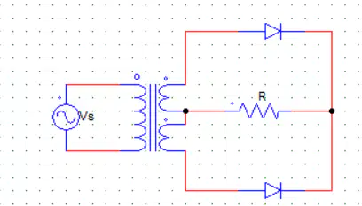
The shown circuit is that of a
Half wave rectification
Center tapped full wave rectification
Bridge rectifier
Bridge rectifier is an alternative for
Half wave
Power rectifier
Full wave rectifier
Peak rectifier
In a full wave rectifier, if the input frequency is 50 Hz, then output frequency will be
50Hz
75Hz
100Hz
25Hz
The electrical resistance of the depletion layer is large because
It has a large number of charge carriers
It has no change carriers
It contains electrons as charge carriers
It has holes as charge carriers
If the forward voltage in a semiconductor diode is doubled, the width of the depletion layer will
Become one-fourth
Remain unchanged
Become half
Become double
When a PN junction diode is reverse biased
Electrons and holes move away from the junction depletion region
Electrons and holes are attracted towards each other and move towards the depletion region
Height of the potential barrier decreases
No change in the current takes place
In the depletion region of an unbiased PN junction diode there are
Only holes
Only fixed ions
Only electrons
Both electrons and holes
On increasing the reverse bias to a large value in a PN junction diode, current
Remains fixed
Decreases slowly
Increases slowly
Suddenly increases
In the breakdown region zener diode acts as .................. source
constant current
constant resistance
constant voltage
None of these
The disadvantage of half wave rectifier is .............
Expensive
Diodes must have high power rating
Output is difficult to filter
None of these
If the temperature of a diode increases, then leakage current ………..
remains the same
increases
decreases
becomes zero
The knee voltage of a diode is approximately equal to ………….
applied voltage
forward voltage
breakdown voltage
barrier potential

