
 Worksheets
Learning Outcomes
Total questions: 83
Worksheet time: 42mins
Electron Sea Model & Band Theory of Metal can be explained as:
Models describing the behavior of electrons in metals and their electrical conductivity.
Models explaining the structure of ionic compounds.
Theories about the bonding in covalent molecules.
Concepts related to the formation of alloys.
A semiconductor is best described as:
A material with electrical conductivity between that of a conductor and an insulator.
A material that does not conduct electricity at all.
A material that conducts electricity perfectly.
A material that only conducts electricity at absolute zero.
What is the definition of a metallic bond?
A force that holds atoms together in a metallic substance.
A force that holds ions together in an ionic compound.
A force that holds molecules together in a covalent compound.
A force that holds protons and neutrons together in the nucleus.
The attraction in a metallic bond is between which two components?
Positive ions and the sea of delocalized electrons.
Negative ions and positive ions.
Atoms and molecules.
Protons and neutrons.
Metallic bonds have strong bonds.
True
False
The strength of a metallic bond is proportional to the number of ______ and inversely proportional to the ______ of the atom.
valence electrons; size
core electrons; mass
protons; charge
neutrons; density
Why is the metallic bond in Mg stronger than in Na?
Because Mg atom has 2 valence electrons and is smaller, while Na has only one valence electron and is larger.
Because Na atom has more protons than Mg atom.
Because Mg atom is larger and has fewer valence electrons than Na atom.
Because both Mg and Na have the same number of valence electrons.
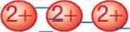
Based on the diagram, as the number of outer-shell electrons increases, what happens to the melting and boiling point?
They increase.
They decrease.
They remain the same.
They fluctuate unpredictably.
What type of solids can metals form by transferring electrons to nonmetals?
Covalent solids
Ionic solids
Metallic solids
Molecular solids
Experiments with metals in the gas phase show that two metal atoms can share their valence electrons to form gaseous, diatomic molecules, such as _____
Na₂
NaCl
NaO
NaF
Atoms in metallic elements are packed closely as possible.
True
False
As a result, valence electrons of each atom become attracted to the positively charged nuclei of the neighbor and become free from the attraction of its own nucleus.
True
False
These free electrons are said to be delocalized over the entire solid embedded in a sea of electron.
True
False
The electron-sea is acting as glue holding the positive ions.
True
False
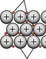
Refer to the diagram labeled 'free electrons from outer shells of metal atoms'. What do the small red dots represent?
Metal ions
Free electrons
Nuclei
Covalent bonds
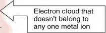
In the diagram showing 'Positive ions from the metal' and 'Electron cloud that doesn't belong to any one metal ion', what does the electron cloud represent?
The electron cloud represents delocalized electrons that do not belong to any one metal ion.
The electron cloud represents protons that are shared between metal ions.
The electron cloud represents neutrons that are free to move within the metal.
The electron cloud represents positive ions that are fixed in place.
Delocalized electrons move freely through bands formed by overlapping MO.
True
False
Used the concept of orbital & based on the modern MO.
True
False
It explains that metals are good conductors, as they are capable of conducting electric current.
True
False
Fill in the blank: The band of orbitals that are filled or partially filled by valence electron is called the _________.
Valence Band
Conduction Band
Forbidden Band
Energy Band
Fill in the blank: The unoccupied bands in which electrons are free to migrate are called the _________.
Conduction Band
Valence Band
Forbidden Band
Energy Gap
Fill in the blank: The energy difference between the valence and conduction band is called the _________.
Band Gap
Work Function
Fermi Level
Electron Affinity
According to the Band Theory of Metal, what is the characteristic of the band gap in insulators?
Large band gap between the valence and conduction band
Small band gap between the valence and conduction band
Overlap between the valence and conduction band
No band gap
According to the Band Theory of Metal, what is the characteristic of the band gap in semiconductors?
Large band gap between the valence and conduction band
Small band gap between the valence and conduction band
Overlap between the valence and conduction band
No band gap
According to the Band Theory of Metal, what is the characteristic of the band gap in conductors?
Large band gap between the valence and conduction band
Small band gap between the valence and conduction band
Overlap between the valence and conduction band
No band gap
Fill in the blank: In insulators, there is a ______ band gap between the valence and conduction band according to the Band Theory of Metal.
large
small
zero
narrow
Fill in the blank: Current flows when electrons move from the _______ band to the conduction band / highest occupied MO to the lowest unoccupied MO.
valence
conduction
forbidden
atomic
Fill in the blank: The amount of _______ required to promote these will determine how well the substance conducts.
energy
pressure
volume
temperature
Fill in the blank: In metal, the _______ band & conducting band are adjacent to each other.
valence
forbidden
energy gap
insulator
Electrons can travel freely through the metal from the valence band to the conduction band.
True
False
Doped Semiconductors: By controlling the number of valence electrons through the creation of specific types of crystal defects, chemists and engineers can greatly increase the conductivity of a semiconductor. What is the main purpose of doping a semiconductor?
To decrease conductivity
To increase conductivity
To change color
To make it magnetic
The most widely used photodetector for general light detection applications is a semiconductor diode with a junction that is accessible to light exposure, called a ________.
photodiode
phototransistor
solar cell
LED
The simplest diode consists of the junction of a p-doped (p-type) and an n-doped (n-type) semiconductor.
True
False
What is a semiconductor?
A material with high conductivity
A material with intermediate conductivity between a conductor and an insulator
A material with no conductivity
A material that only resists electron flow
Which property allows a semiconductor to resist and allow the flow of electrons depending on the energy applied?
Conductivity
Insulation
Variable resistance
Superconductivity
Semiconductors are commonly used in electronics as ________ or diodes.
transistors
resistors
capacitors
inductors
What is the process called wherein impurities are added to a semiconductor to improve its conductivity?
Mixing
Doping
Alloying
Insulating
Which is the most commonly used semiconductor material?
Germanium
Silicon
Copper
Gold
What are the two types of semiconductors formed by doping?
A) P-Type and N-Type
B) A-Type and B-Type
C) X-Type and Y-Type
D) S-Type and T-Type
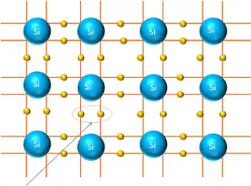
In the diagram showing sharing of electrons, which element is represented by the blue circles?
Carbon
Silicon
Germanium
Oxygen
What type of semiconductor naturally has a moderate band gap?
Intrinsic Semiconductor
Extrinsic Semiconductor
Metallic Semiconductor
Superconductor
A small fraction of the electrons in the valence band can be excited into the conduction band. They can carry current. This property is associated with which type of semiconductor?
Intrinsic Semiconductor
Extrinsic Semiconductor
Compound Semiconductor
Degenerate Semiconductor
Which type of semiconductor has had impurities added in order to increase the amount of current they can conduct?
Extrinsic Semiconductor
Intrinsic Semiconductor
Superconductor
Insulator
The dopants in extrinsic semiconductors can either provide extra electrons or provide extra holes.
True
False
A semiconductor doped to have extra electrons is called what type of semiconductor? (n is for 'negative')
n-type semiconductor
p-type semiconductor
intrinsic semiconductor
photo semiconductor
A semiconductor doped to have extra holes is called what type of semiconductor?
p-type semiconductor
n-type semiconductor
intrinsic semiconductor
photo-conductive semiconductor
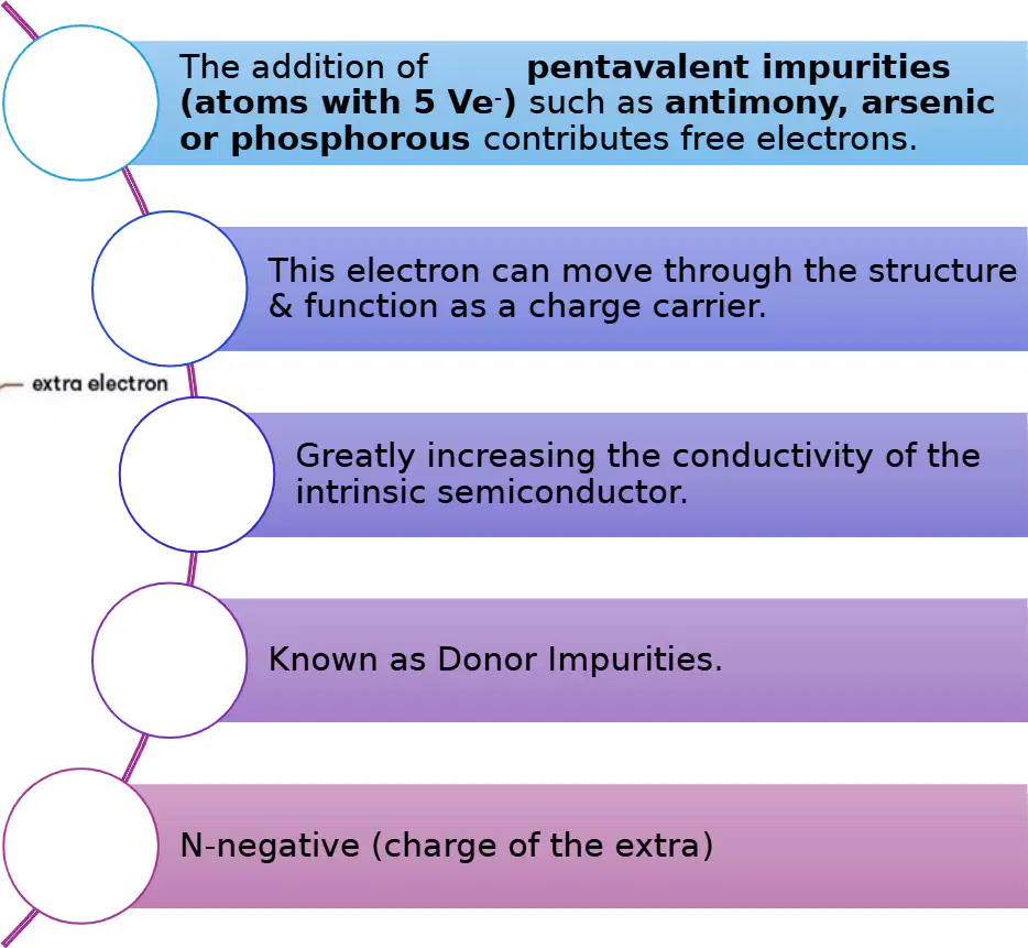
What type of impurities are added to create an N-type semiconductor?
Trivalent impurities
Pentavalent impurities (atoms with 5 Ve-) such as antimony, arsenic or phosphorous
Divalent impurities
Monovalent impurities
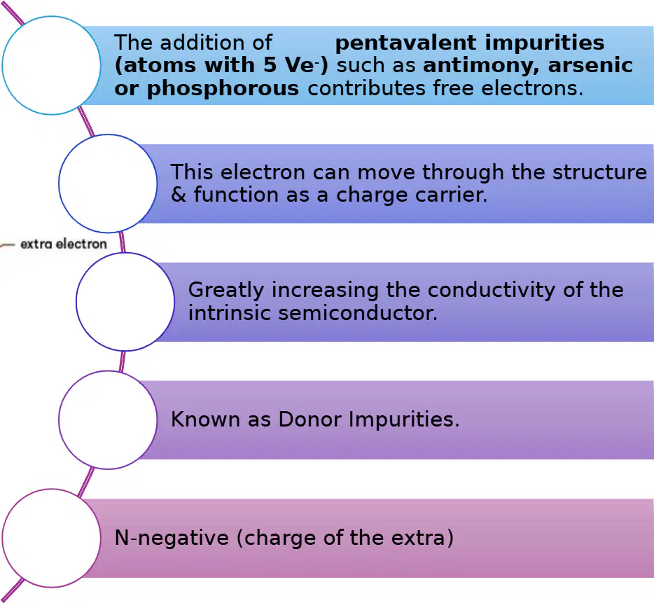
What is the role of the extra electron in an N-type semiconductor?
This electron can move through the structure & function as a charge carrier.
It remains fixed and does not participate in conduction.
It creates holes in the valence band.
It neutralizes the positive ions in the lattice.
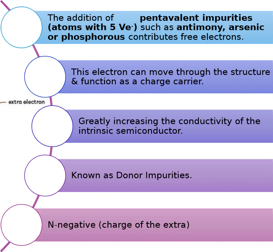
The addition of pentavalent impurities in a semiconductor greatly increases the ________ of the intrinsic semiconductor.
conductivity
resistance
band gap
melting point
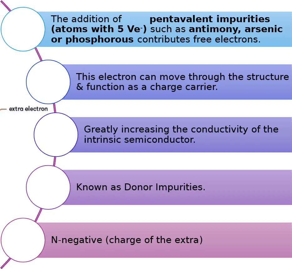
What are N-type impurities also known as?
Acceptor Impurities
Donor Impurities
Neutral Impurities
Negative Impurities
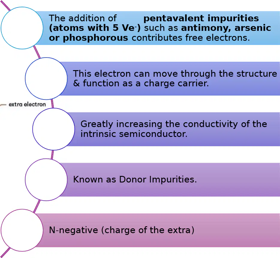
The charge of the extra electron in an N-type semiconductor is:
Positive
Negative
Neutral
Both positive and negative

Which type of impurities are added to create a P-type semiconductor?
Monovalent impurities
Divalent impurities
Trivalent impurities (atoms with 3 Ve-) such as boron, aluminum, or gallium
Pentavalent impurities

The addition of trivalent impurities creates deficiencies of ________ called 'holes'.
valence electrons
protons
neutrons
conduction electrons

In a P-type semiconductor, the charge carrier is effectively a:
Negatively charged electron
Positively charged hole
Neutral atom
Negatively charged ion

What are acceptor impurities known as in a P-type semiconductor?
Acceptor impurities
Donor impurities
Intrinsic impurities
Neutral impurities

P-type semiconductors are also called:
N-negative (electrons)
P-positive (holes)
Neutral semiconductors
D-type semiconductors
What is the main difference between the extra energy levels in N-Type and P-Type materials?
N-Type has extra electron energy levels, P-Type has extra hole energy levels
N-Type has extra hole energy levels, P-Type has extra electron energy levels
Both have extra electron energy levels
Both have extra hole energy levels
In n-type material, there are electron energy levels near the top of the band gap so that they can be easily excited into the conduction band.
True
False
In p-type material, extra holes in the band gap allow excitation of valence band electrons, leaving mobile holes in the valence band.
True
False
Fill in the blank: In N-Type material, the extra energy levels are for _________.
electrons
holes
protons
neutrons
Fill in the blank: In P-Type material, the extra energy levels are for _________
holes
electrons
protons
neutrons
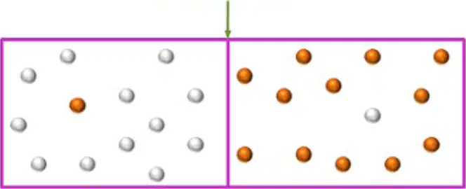
Refer to the diagram of the P-N junction. Which type of semiconductor has holes as majority carriers?
A) P-type
B) N-type
C) Both
D) None
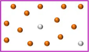
In the diagram, which region contains free electrons as majority carriers?
P-type
N-type
Both
None
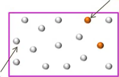
Fill in the blank: In a P-type semiconductor, the majority charge carriers are _______.
holes
electrons
protons
neutrons
Fill in the blank: A ________ is an example of a semiconductor.
Micro controller
Resistor
Capacitor
Transformer
A ________ is an example of a semiconductor.
Memory card
Wooden block
Glass bottle
Rubber band
Fill in the blank: ________ are used as display drivers and are examples of semiconductors.
Display drivers
Resistors
Capacitors
Inductors
Fill in the blank: ________ are used as audio drivers and are examples of semiconductors.
Audio drivers
Capacitors
Resistors
Inductors
Fill in the blank: A ________ controller is an example of a semiconductor.
Keyboard
Fan
Light Bulb
Speaker
Fill in the blank: A ________ is a type of semiconductor device.
Transistor
Resistor
Capacitor
Inductor
Fill in the blank: A ________ is a type of semiconductor device.
Diode
Resistor
Capacitor
Transformer
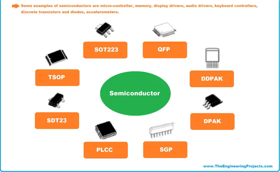
Which of the following is a type of semiconductor package?
SOT223
QFP
DDPak
All of the above
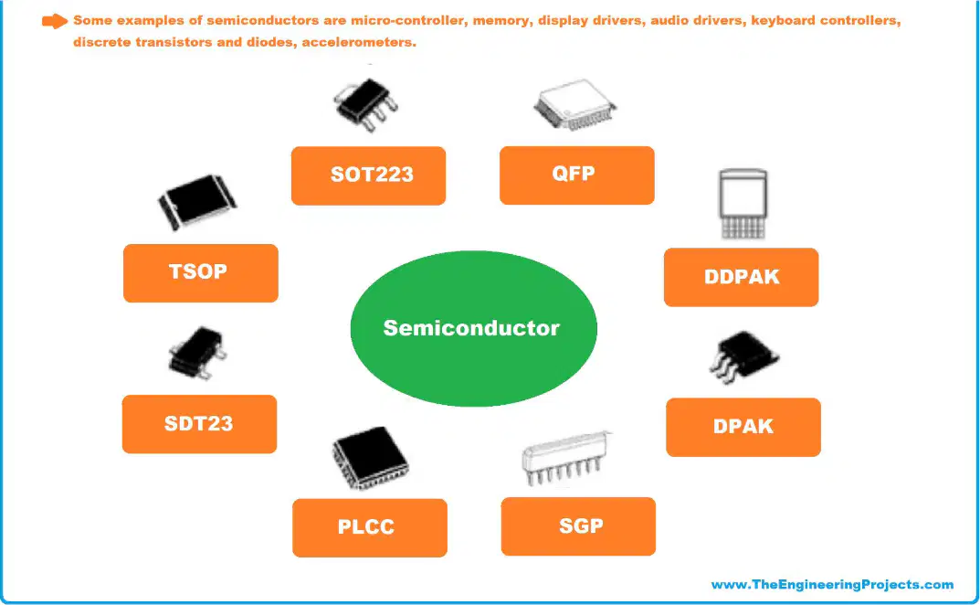
Which of the following is NOT listed as a semiconductor package type?
SOT223
QFP
DDPak
Capacitor

Fill in the blank: ________ is a type of semiconductor package shown in the diagram.
TSOP
DIP
QFP
BGA

Fill in the blank: ________ is a type of semiconductor package shown in the diagram.
SDT23
TO-220
DIP-8
QFN

Fill in the blank: ________ is a type of semiconductor package shown in the diagram.
PLCC
BGA
DIP
QFP

Fill in the blank: ________ is a type of semiconductor package shown in the diagram.
SGP
DIP
QFP
BGA

Fill in the blank: ________ is a type of semiconductor package shown in the diagram.
DPAK
TO-220
SOT-23
QFN

Fill in the blank: ________ is a type of semiconductor package shown in the diagram.
DDPAK
TO-220
SOT-23
QFN
Fill in the blank: The application of a Diode in P-N type semiconductors is __________.
Light-Emitting Diodes (LEDs)
Capacitors
Transformers
Resistors
Fill in the blank: The application of Solar Cells in P-N type semiconductors is __________.
photovoltaic technology
thermoelectric generation
piezoelectric effect
electrolysis
Fill in the blank: The application of Photodetectors in P-N type semiconductors is __________.
sensors and cameras
power generation
audio amplification
mechanical support
Fill in the blank: The application of Laser Diodes in P-N type semiconductors is __________.
laser pointers, optical storage devices (like CD and DVD players), and fiber optic communications
heating elements in electric stoves
mechanical relays in circuits
display screens in televisions

