
NEW
Font size
 Worksheets
Quiz on Digital E and Basic E
Total questions: 40
Worksheet time: 19mins

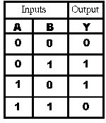
Which Logic gate does this Truth Table represent?
AND Gate
OR Gate
NOT Gate
NAND Gate
NAND Gate is called a universal logic element, because
It is used by everybody
Any logic function can be realised by NAND Gate alone
Many digital computers use NAND Gate
All the minimisation techniques are applicable to optimum NAND Gate realisation
Which are the UNIVERSAL GATES?
XOR Gate & NOT Gate
AND Gate & OR Gate
NAND Gate & NOR Gate
All of the above
The two inputs of a NAND gate are both low (logic level 0). The output state is...
1
0
symbol for a NOT gate?


The base of octal number is
2
8
10
11
The number 15 is represented as ............in Hexadecimal.
C
E
F
D
The number 5A6D belongs to which category of number system
Octal
Hexadecimal
Binary
DEcimal
3) The boolean expression of an OR gate is _______
a) A.B
b) A’B+AB’
c) A+B
d) A’B’
Which of the following statements is TRUE for an OR Gate:
A '1' at any of the inputs causes the output to be '1'
A '1' at any of the inputs causes the output to be '0'
A '0' at any of the inputs causes the output to be '0'
A '0' at any of the inputs causes the output to be '1'
The inputs of a NAND Gate are connected together. The resulting circuit is .............
AND Gate
OR Gate
NOT Gate
None of the above

What type of Flip-Flop is pictured here?
J-K
D
S-R
Toggle
A circuit with one input and many outputs
Multiplexer
Demultiplexer
None of the above
One's compliment of 1011
0101
1000
0100
Binary equivalent of 1310
1101
1111
1010
Decimal equivalent of (1100)2
10
12
8
If A, B and C are the inputs of a full adder then the sum is given by __________
A AND B AND C
A OR B AND C
A XOR B XOR C
A OR B OR C
If A and B are the inputs of a half adder, the sum is given by __________
A AND B
A OR B
A XOR B
A EX-NOR B
Total number of inputs in a half adder is __________
1
2
4
3
The logic circuits whose outputs at any instant of time depends only on the present input are called ________________
a) Combinational circuits
b) Sequential circuits
c) Latches
d) Flip-flops
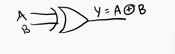
Identify the name of this gate
NAND Gate
NOR Gate
X-OR Gate
Ex-NOR Gate
To work as a Amplifier, the transistor has to be operated in
Cut off region
Saturation region
Active region
All of the above
In CB configuration, the value of α is
IEIC
IBIE
ICIB
ICIE
The efficiency of a centre-tapped full wave rectifier is;
50%
46%
70%
81.2%
Addition of pentavalent impurity to a semiconductor creates _____.
Free Electrons
Holes
Valence Electrons
Valence Ion
Relation between Alpha and Beta is
α=1+β
β=α−1
β=1−αα
α=1−ββ
Vdc in halfwave rectifier
2Vm
2Vm
πVm
πVm
The maximum amount of reverse voltage which can be applied on a diode before breakdown is reached
Zener Voltage
Peak Inverse Voltage
Breakdown Voltage
Threshold Voltage
In a Transistor ………………..
IE = IC + IB
IC = IE + IB
IE = IC – IB
IB = IC + IE
The Base – Emitter Diode (Base – Emitter Junction) in an NPN Transistor is
A. Doesn’t conduct
B. Forward Biased
C. Reverse Biased
D. Operates in breakdown region
In transistors conduction occurs due to the flow of
Minority charge carriers
Majority charge carriers
Both majority and minority charge carriers
The base region of a transistor is doped:
Heavily
Moderately
Lightly
None of the above
The net charge of an N-type semiconductor is
Negative
Zero
Positive
Dependent
A semiconductor in its purest form is called.......
Extrinsic semiconductor
Superconductor
Intrinsic semiconductor
Insulator
The depletion layer of a PN junction diode has
Only free mobile holes
Only free mobile electrons
Both free mobile holes as well as electrons
Neither free mobile electrons nor holes
The color of light emitted by a LED depends on
its forward bias
its reverse bias
the amount of forward current
the type of semiconductor material used
The advantage of LED is
Long life
Fast on-off switching
Low operating voltage
All of the above
The potential difference created across the P-N junction due to the diffusion of electrons and holes is called___________
back emf
depletion voltage
barrier potential

