
 Worksheets
GEM of DEMP
Total questions: 52
Worksheet time: 35mins
WHICH NUMBER SYSTEM IS USED BY COMPUTER FOR INTERNAL CALCULATION
DECIMAL
BINARY
NUMBER SYSTEM WHOSE BASE IS 8
DECIMAL
BINARY
OCTAL
TO CONVERT DECIMAL TO OCTAL NUMBER WE HAVE TO
SUBTRACT BY 8
MULTIPLY BY 8^0
DIVIDE BY 8
OX345 THIS NUMBER IS REPRESENTED IN
OCTAL
HEXA
DECIMAL
LETTER 'C' IN HEXA REPRESENTS
12
13
11


A four variables Karnaugh map contains
4 cells
8cells
16 cells
32 cells
A five variables Karnaugh map contains
4 cells
8 cells
16 cells
32 cells
AND-OR realisation is equivalent to
SOP
POS
K-MAP
Boolean function
A combinational circuit has 3 inputs A, B, C and output F. F is true for following input combinations,
(i) A is False, B is True
(ii) A is False, C is True
(iii) A, B, C are False
(iv) A, B, C are True
Find the simplified expression for F in SOP form.
F = A+BC
F = A’+B'C'
F = A’+BC
F = A+B'C'

The Karnaugh map for a SOP function is given below in Fig.1. Determine the simplified SOP Boolean expression.
F = BD+B'C'+A'C'D
F = B'D'+BC+A'C'D
F = B'D'+B'C'+ACD
F = B'D'+B'C'+A'C'D
A minterm is
The minimum term in a Boolean function
A prime implicant
A square on a karnaugh map
Always smaller than a maxterm
is the same as
A + B + C

Write the output expressions for the following logic gate combinations:
(ABC) + (DE)
(ABC)(DE)
(ABC) X (DE)
(ABCDE)
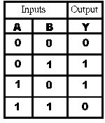
Design a combinational circuit with three inputs and one output. The output is 1 when the binary value of the inputs is less than 3. The output is 0 otherwise.
F = x'y' + x'z
F = x'y + x'z
F = x'y' + xz
F = x'y' + x'z'
The combinational circuit which converts a decimal number into its equivalent binary code is ___________.
Decoder
DEMUX
Encoder
MUX
In general, Encoder has
n inputs, 2n inputs
n inputs, 2^n inputs
2n inputs, n outputs
2^n inputs, n outputs
10 line to 4 line Encoder is also known as _______________ Encoder.
Decimal to BCD
Hexadecimal to Decimal
Octal to BCD
BCD to Decimal
The BCD number 101011 has _______ priority.
Even
Odd
Both even and odd
Undefined
Multiplexer is a ____ logic circuit
Combinational
Sequential
Random
Memory
A full
adder has __________ inputs & ___________ outputs.
2, 2
3, 2
2, 3
2,1
Which
gate is best used as a basic comparator?
NOR
OR
Exclusive-OR
AND

1. Choose the correct one from among the alternatives A, B, C, D after matching an item from Group 1 with the most appropriate item in Group 2.
P – 3, Q – 2, R – 1
P – 3, Q – 1, R – 2
P – 2, Q – 1, R – 3
P – 1, Q – 2, R – 2
What is/are the directional mode/s of shifting the binary information in a shift register?
Up-Down
Left - Right
Front - Back
All of the above
Sequential circuit includes
only Delays
Only Feed backs
Delays and Feed backs from input to output
Delays and Feed backs from output to input
Which of the listed flip-flops is also known as a programmable flip-flop?
Clocked SR flip-flop
T-type flip-flop
JK flip-flop
D-type flip-flop
What type of register would shift a complete binary number in one bit at a time and shift all the stored bits out one bit at a time?
PIPO
SIPO
PISO
SISO
In a simple low activated SR flip-flop, the Q and NOT Q will be indeterminate (unknown) if:
Both S and R are at logic 0 together
Both S and R change from logic 0 to logic 1 together
R changes to logic 0 while S is at logic 1
S changes to logic 0 while R is at logic 1
Memory size of 8086 microprocessor
1MB
4KB
256 bytes
128bytes
The number of General Purpose Registers present in 8086 microprocessor
4
14
10
34
The starting address of the segment is called
base address
offset address
effective address
none of the above
After using Shift Arithmetic Right instruction the BL register containing 10101001 becomes
11010100
01010011
1. A microcontroller at-least should consist of:
RAM, ROM, I/O ports and timers
CPU, RAM, I/O ports and timers
CPU, RAM, ROM, I/O ports and timers
CPU, ROM, I/O ports and timers
4. If we say microcontroller is 8-bit then here 8-bit denotes size of:
Data Bus
ALU
Control Bus
Address Bus
6. Abbreviate CISC and RISC.
Complete Instruction Set Computer, Reduced Instruction Set Computer
Complex Instruction Set Computer, Reduced Instruction Set Computer
Complex Instruction Set Computer, Reliable Instruction Set Computer
Complete Instruction Set Computer, Reliable Instruction Set Computer
10. Why microcontrollers are not called general purpose computers?
because they have built in RAM and ROM
because they design to perform dedicated task
because they are cheap
because they consume low power
The bus is available when the DMA controller receives the signal
HRQ
HLDA
DACK
All of the mentioned
The number of clock cycles required for an 8257 to complete a transfer is
2
4
8
NONE
All the functions of the ports of 8255 are achieved by programming the bits of an internal register called
data bus control
read logic control
control word register
none of the mentioned
Which of the following is not a Features of 8086?
It uses two stages of pipelining
It is available in 3 versions based on the frequency of operation
Fetch stage can prefetch up to 6 bytes of instructions
It has 512 vectored interrupts.
8086 can access up to?
512KB
1Mb
2Mb
256KB
. 8085 microprocessor is an 8-bit microprocessor designed by?
IBM
DELL
INTEL
MOTOROLA

