
 Worksheets
Leji sesi >.<
Total questions: 108
Worksheet time: 54mins
Name
Class
Date
1.
a)
sdad
b)
asdea 2
2.
a)
as
b)
dasd
3.
a)
dd
b)
ddasd
4.
a)
ab
b)
bfv
5.
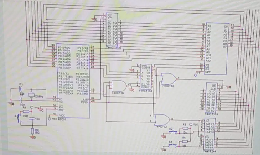
a)
Sistemul are un port de intrare care poate fi citit prin intermediul unei variabile localizate la adresa AD32H.
b)
Circuitul 74HCT373 memoreaza si transmite octetul cel mai putin semnificativ al magistralei de adrese la activarea semnalului ALE.
c)
Circuitul de reset filstreaza salturile de tensiune la apasarea tastei.
d)
Sistemul are un port de iesire care poate fi scris prin intermediul unei variabile localizate la adresa 823DH.
e)
Sistemul are un port de iesire care poate fi scris prin intermediul unei variabile localizate la adresa 2AE6H.
6.
Despre marginile de zgomot ale portii fundamentale SI-NU construita in tehnologie TTL, se pot afirma urmatoarele: (4 raspunsuri)
a)
Valoarea garantata a marginii de zgomot pentur "0" logic este de 0.4V.
b)
Valoarea garantata a marginii de zgomot pentru "0" logic este egala cu valoarea garantata a marginii de zgomot pentru "1" logic.
c)
Valoarea reala a marginii de zgomot pentru "0" logic depaseste valoarea garantata pentru aceeasi stare logica.
d)
Marginile reale de zgomot explica preferinta ca starea de inalta impedanta a unui circuit logic sa fie comandata cu starea logica "1".
e)
Valoarea garantata se calucleaza in functie de tensiunea prag.
7.
What components does a microcontroller include? (2 answers)
a)
Keyboard
b)
Memory
c)
Power supply
d)
Counter
8.

Consider the 80C51 microcontroller system in the figure. Which statements are correct? (4 answers)
a)
The system has an input port that can be read through a variable located at address C237H.
b)
The system has an output port that can be written through a variable located at address 41B7H.
c)
The partial selection is used to activate the input port.
d)
The clock generator circuit consists of both external components of the microcontroller and components integrated in it.
e)
The total selection is used to activate the input port.
9.
Which bus is bidirectional?
a)
None
b)
Address bus
c)
Address and data bus
d)
Data bus
10.
Forward switching time is:
a)
The necessary time for a transistor to switch from the conduction state to the cut-off state.
b)
The necessary time for a transistor to switch from the normal state to the reverse state.
c)
The necessary time for a transistor to switch from the cut-off state to the conduction state.
11.
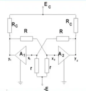
Consider the general diagram of a flip-flop circuit. Select the correct statement:
a)
Resistors R and r form a voltage divider.
b)
Amplifiers A1 and A2 are connected in negative reaction.
c)
The circuit is asymmetric.
d)
The circuit is monostable.
12.
The possible roles of a three state circuit are: (2 answers)
a)
Bus driver
b)
Decoding addresses on the address bus
c)
NO gate for Chip Select inputs of integrated circuits
d)
To connect multiple data sources to the same bus
13.
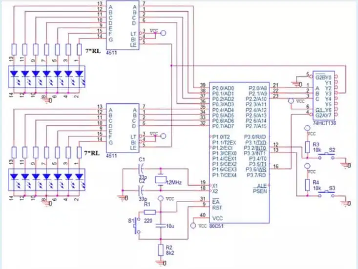
Consider the 80C51 microcontroller system in the figure. Which statements are correct? (3 answers)
a)
We know that for IOH =10mA, circuit 4511 has VOHtyp = 4.25V. For VLED = 2V and ILED = 10mA, the approximative value of the RL resistor through which the LED is controlled will be 225 Ohm.
b)
The microcontroller uses only the internal program memory.
c)
The clock generator circuit consists of both external components of the microcontroller and components integrated in it.
d)
We know that for IOH =10mA, circuit 4511 has VOHtyp = 4.25V. For VLED = 2V and ILED = 10mA, the approximative value of the RL resistor through which the LED is controlled will be 100 Ohm.
e)
The microcontroller uses only the external program memory.
14.
Semiconductor diode - at thermal equilibrium: (1 answer)
a)
The electric current will best pass through the semiconductor
b)
The electric current will partially pass through the semiconductor
c)
The semiconductor acts as a low value resistor (Ohm)
d)
Electric current will not be produced at all through semiconductor
15.
When interconnecting logic circuits: (2 answers)
a)
Fan-in (FI) and Fan-Out (FO) factors are defined as voltage levels in the admitted or guaranteed range
b)
The value of the output current of the control circuit must be less than the sum of the input currents of the controlled circuits
c)
The value of the output current of the control circuit must be at least equal to the sum of the input currents of the controlled circuits
d)
The Fan-out (FO) factor of an output is defined as the minimum of the FO factors of the outputs of logic levels "0" and "1"
e)
The Fan-in (FI) factor of an input is less than 1
16.
Which statements are true for memory circuits based on SRAM CMOS memory cell? (2 answers)
a)
Integration capacity is higher than in case of DRAM circuits
b)
They need refresh circuits
c)
The integration capacity is lower than in the case of DRAM circuits
d)
There is no need for refresh circuits
e)
They need comparison circuits
17.
What happens when the threshold voltage Vt is exceeded at an NMOS transistor?
a)
The concentration of electrons in the channel area between the drain and the substrate will exceed the concentration of holes and then the region will change its type, form p type to n type.
b)
The concentration of electrons in the channel area between the drain and the source will exceed the concentration of holes and then the region will change its type, form p type to n type.
c)
The concentration of electrons in the channel area between the drain and the source will exceed the concentration of holes and then the region will change its type, form n type to p type.
18.
If a second interrupt is activated during the execution of an interrupt (with a different priority level), what is the behavior of the microcontroller?
a)
The interrupt with higher priority is executed, only if they are triggered simultaneously, otherwise the execution of the current interrupt is continued.
b)
The interrupt with higher priority is always expected.
c)
The execution of the current interrupt is continued, regardless of the priority level of the two interrupts.
d)
The newest interrupt is always executed.
19.
What is the usual method of selecting memory cells in an integrated circuit?
a)
Based on the coincidence of the horizontal and vertical selection.
b)
Based on the address sent on the data lines.
c)
Based on the dedicated address generation circuit.
d)
Based on the select chip line.
20.
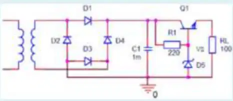
Consider the reaction stabilizer with no error amplifier in the figure, where the Zener diode threshold voltage is 5.6V and Vout represents the output voltage: (2 answers)
a)
If the output voltage decreases, the resistance between the collector and the emitter of transistor decreases.
b)
If we measure 0.4V on Vbe, the Vout voltage will be 5.1V.
c)
If we measure 5.1V on Vout, the Vbe voltage will be 0.5V.
d)
If the output voltage decreases, the resistance between the collector and the emitter of the transistor increases.
e)
If we measure 5.1V on Vout, the Vbe voltage will be 5.7V.
21.
The characteristics of operational amplifiers are: (3 answers)
a)
Very high input impedance (ideal infinity).
b)
Very small input currents (ideal 0).
c)
Output voltage is bounded by power supplies values.
d)
Very small amplification or voltage gain (AV) (ideal 0).
e)
Very small input impedance (ideal 0).
22.
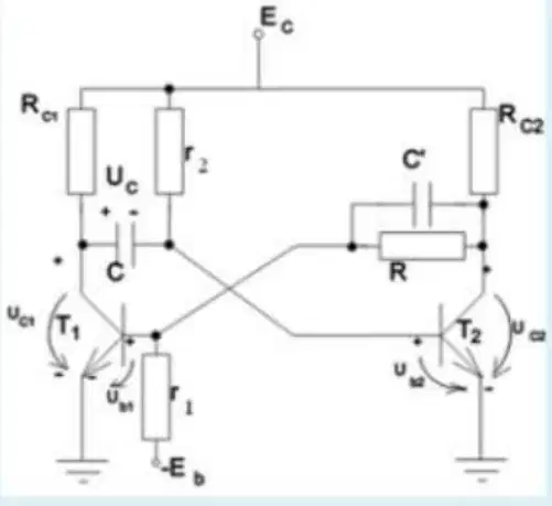
The monostable circuit in the picture is considered. (2 answers)
a)
Capacitor C controls the blocking of transistor T2 if the voltage UC1 drops rapidly.
b)
The circuit is symmetrical.
c)
The transistor T2 at saturation, determines the increase of voltage on the base of T1 transistor by discharging the capacitor C.
d)
The circuit can have two states, one stable and one unstable.
23.
In the case of Wien Bridge oscillator: (2 answers)
a)
The positive feedback loop allows the occurrence and increase of the amplitude of the oscillations.
b)
The positive feedback loop determines the oscillation frequency.
c)
The control signals are rectangular.
d)
The negative feedback loop determines the oscillation frequency.
e)
The negative feedback loop allows the occurrence and increase of the amplitude of the oscillations.
24.
CMOS inverter static transfer characteristic...(3 answers)
a)
Depends on the supply voltage.
b)
Depends on the threshold voltage of the transistor Mp.
c)
Depends on the threshold voltage of the transistor Mn.
d)
Depends on the number of gates driven by the inverter.
e)
Depends on the maximum frequency at which the circuit can operate.
25.
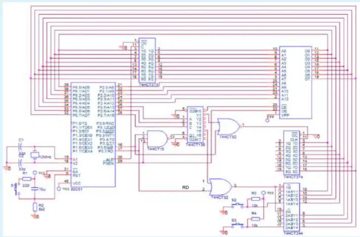
Consider the 80C51 microcontroller system in the figure. Which statements are correct? Select one or more: (4 answers)
a)
The system has an input port that can be read through a variable located at address A187H.
b)
The reset circuit ensures a logic level 0 at the input pin of the microcontroller if the key is not pressed.
c)
The clock generator circuit consists of both external components to the microcontroller and components integrated in it.
d)
The partial selection is used to activate the input port.
e)
The system has an input port that can be read through a variable located at address C1A3H.
26.
Check the correct option for the high-pass and low-pass filters:
a)
The high-pass filter attenuates the low frequencies and less alters the high frequencies.
b)
The dividing ratio depends on the frequency only for the high-pass filter.
c)
The capacitive reactance of the capacitor decreases as the period increases.
d)
In both filters, the distortions introduced by the circuit on the input signal be reduced if the time constant RC is greater than the pulse duration.
27.
What are light emitting diodes?
a)
Diodes that when forward biased, the electrons in the n region recombine with the holes in the p region and release energy in the form of light and heat.
b)
There are diodes that allow the passage of current in both directions and have the role of increasing the resistance of the circuit.
c)
Diodes that, upon reverse polarization, in the n region, release energy in the form of light and heat.
28.
Regarding the currents of the fundamental NAND gate built in TTL technology, the following can be stated:
a)
The gate absorbs current at the output when it commands with logic "1" level.
b)
The gate absorbs current at the input when it is controlled with logic "0" level.
c)
The gate generates output current when it is commands with logic "0" level.
d)
The gate generates current at the input when it is controlled with logic "0" level.
e)
The gate cannot absorb current at the output.
29.

a)
d
b)
s
30.
Check the correct option(s) for the high-pass and low-pass filters: (1 answer)
a)
The low-pass filter attenuates the low frequencies and less alters the high frequencies.
b)
If we apply a sinusoidal signal to either of the two filters, the response is still sinusoidal, only attenuated and out of phase.
c)
The capacitive reactance of a capacitor increases as the period decreases.
d)
The dividing ratio depends on the frequency only for the low-pass filter.
31.
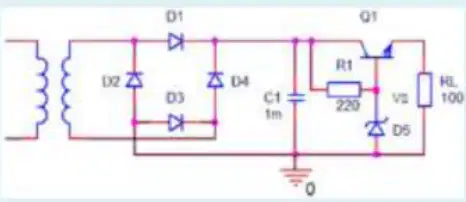
Consider the reaction stabilizer with no error amplifier in the figure, where the Zener diode threshold voltage is 5.6V and Vout represents the output voltage: (2 answers)
a)
If we measure 5.0V on Vout, the Vbe voltage will be 0.6V.
b)
If we measure 4.9V on Vout, the Vbe voltage will be 5.5V.
c)
If we measure 0.5V on Vbe, the Vout voltage will be 5.0V.
d)
The circuit regulates the voltage only if RL doesn't change its value.
e)
The circuit regulates the voltage even if RL changes its value.
32.
a)
a
b)
v
33.
a)
a
b)
c
34.

Consider the Rs flip-flop circuit in the picture. Select the correct statement:
a)
In the state T1 = saturated and T2 = blocked, the applying of a pulse at the input S determines the blocking of the transistor T1.
b)
Diode D1 allows the passage of signals applied to the cathode if the voltage is positive and high enough.
c)
By using capacitor C1 and C2 it is ensured that diodes D1 and D2 will recieve only positive signals on the cathode.
d)
By applying a pulse to input S, the circuit R2C2 generates a signal with a negative voltage peak.
35.
Check the correct options for the pulse: (2 answers)
a)
For digital signals, if the filling factor is 50%, the repetition period is twice the pulse duration.
b)
To correctly define the pulse repetition period, the duration of the transitory regime in the circuit must be less than this period.
c)
To correctly define the pulse repetition period, the duration of the transitory regime in the circuit must be longer than this period.
d)
The filling factor is always half the repetition period.
36.
For CAM memories the matching signals: (1 answer)
a)
Logic state '1' indicates that no stored bit corresponds to the searched bit
b)
Indicates whether the match between the searched and the stored word was found
c)
Are stored in memory instead of existing data
d)
Logic state '0' indicates that a stored bit corresponds to the searched bit
37.
Regarding the Fan-in (FI) and Fan-out (FO) factors of the fundamental NAND gate built in TTL technology, the following can be stated: (2 answers)
a)
The FI factor for "0" is less than 1.
b)
The FI factor is calculated based on the input currents.
c)
Based on the FI and FO, a NAND gate implemented in TTL tech. can drive at least 20 NAND gates of the same type.
d)
The value of the FO factor represents the maximum number of gates that can be driven by the NAND gate.
38.
Coupling the outputs of two TTL or CMOS gates, with usual structure, in parallel, will result in: (2 answers)
a)
Destruction of both gates or one of them.
b)
Changing the gates' parameters.
c)
Proper operation of one of the two gates.
d)
The common output voltage level can be used in digital system.
39.
Immunity margins to static perturbations of logic integrated circuits: (2 answers)
a)
For "0", it is calculated as the difference between the minimum voltage level for "0" at the input and the maximum for "1" at the input.
b)
For "0", it is calculated as the difference between the maximum voltage level for "0" at the input and the maximum for "0" at the output.
c)
They are also called noise margins.
d)
Cannot be calculated for both logic states "0" and "1".
40.
Immunity margins to static perturbations of logic integrated circuits: (2 answers)
a)
For "1", it is calculated as the difference between the minimum voltage level for "1" at the output and the minimum for "1" at the input.
b)
They are also called noise margins.
c)
Cannot be calculated for both logic states "0" and "1".
d)
For "1", it is calculated as the difference between the minimum voltage level for "1" at the input and the minimum for "1" at the output.
e)
For "1", it is calculated as the difference between the minimum voltage level for "0" at the input and the minimum for "1" at the input.
41.
8051 family microcontrollers can use the UART serial interface in the following ways: (2 answers)
a)
Baud rate inscribed in memory.
b)
Baud rate read through a terminal.
c)
Fixed Baud rate.
d)
Variable Baud rate generated by a timer.
42.
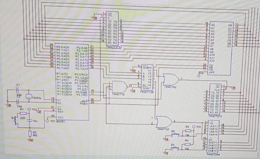
Se considera sistemul cu microcontroller 80C51 din figura. Care afirmatii sunt adevarate? (4 raspunsuri)
a)
Sistemul are un port de intrare care poate fi citit prin intermediul unei variabile localizata la adresa AD32H
b)
Circuitul 74HCT373 memoreaza si transmite octetul cel mai putin semnificativ al magistralei de adrese la activarea semnalului ALE
c)
Circuitul de reset filtreaza salturile de tensiune la apasarea tastei
d)
Sistemul are un port de iesire care poate fi scris prin intermediul unei variabile locale la adresa 2AE6H
e)
Sistemul are un port de iesire care poate fi scris prin intermediul unei variabile locale la adresa B23DH
43.

Considerând valorile ieşirilor din imaginea de mai jos, este adevărat că: (alegeți 1 răspuns)
a)
a. Nivelul tensiunii la ieșirea comună a porţilor este dat de funcţia SI între ieşirile fiecărei porţi.
b)
b. Circuitul funcționeaza fără pierderi.
c)
c. Consumul celor două circuite TTL este redus.
d)
d. Puterea disipată pe rezistența R24 și tranzistorii Q23 și Q14 este prea mare.
44.
Din cate circuite de memorie de 512*8 se obtine un bloc de memorie avand capacitatea de 16384*32(1 raspuns)
a)
a. 80
b)
b. 64
c)
c. 120
d)
d. 128
45.
Tensiunea de prag (Vt) a tranzistorului M este: (1 raspuns)
a)
O valoare a tensiunii grila-drena
b)
O valoare a tensiunii grilei
c)
O valoare a tensiunii sursa-baza
d)
O valoare a tensiunii grila-sursa
46.
Care afirmatii sunt adevarate in cazul circuitelor de memorie bazate pe celula de memorie SRAM CMOS (2 raspunsuri)?
a)
Informatia este stocata in condensatoare
b)
Informatia este stocata in bistabile realizate cu tranzistoare MOS
c)
Informatia este stocata intr un dispozitiv MOS cu stocare de sarcina si poarta flotanta
d)
Celulele de memorie nu trebuie reincarcate dupa fiecare ciclu de citire
e)
Celulele de memorie trebuie reincarcate dupa fiecare ciclu de citire
47.
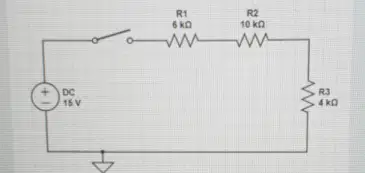
Pentru circuitul de mai jos, calculati caderile de tensiune si curentii prin rezistori:
a)
a. UR1=4.5V, I1 = 0.75mA UR2 =7.5V, I2=0.75mA UR3=3V, I3=0.75mA
b)
b. UR1=5V, I1=1.25mA UR2=8V, I2=1.25A UR3=2V, I3=1.25mA
c)
c. UR1=5V, I1=0.5mA UR2=5V, I2=0.75mA UR3=5V, I3 = 1.5mA
d)
d. UR1=3V, I1=1mA UR2=9V, I2=1mA UR3=3V, I3=1mA
48.
Pe fonturile de comutație ale circuitelor integrate CMOS, puterea disipată...(1 răspuns)
a)
Poarta nu consumă curent
b)
Crește consumul de putere
c)
Toate variantele
d)
Unul dintre cele două tranzistoare MOS complementare este blocat
49.
Cate impulsuri de tact (aproximativ) trebuie sa treaca pentru fiecare bit, in cadrul unei transmisii seriale (e.g. UART), daca se utilizeaza un oscilator cu frecventa de 12MHz si se doreste obtinerea unei rate Baud de 115200 biti pe secunda? (Selectati 1 raspuns):
a)
a. 104
b)
b. 115
c)
c. 75
d)
d. 12
50.
Care afirmații sunt adevărate în cazul circuitelor de memorie bazate pe celula de memorie DRAM MOS cu un tranzistor? (2 raspunsuri)
a)
Celulele de memorie nu trebuie reincarcate dupa fiecare ciclu de citire
b)
Celulele de memorie trebuie reincarcate dupa fiecare ciclu de citire
c)
Informatia este stocata in bistabile realizate cu tranzistoare MOS
d)
Informatia este stocata intr-un dispozitiv MOS cu stocare de sarcina si poarta flotanta
e)
Informatia este stocata in condensatoare
51.
Care afirmații sunt adevărate în cazul circuitelor de memorie bazate pe celula de memorie SRAM CMOS (alegeți 2răspunsuri)?
a)
a. Este o memorie adresabila prin continut
b)
b. Este o memorie nevolatila
c)
c. Este o memorie volatila
d)
d. Operatia de citire nu este distructiva
e)
e. Operatia de citire este distructiva
52.
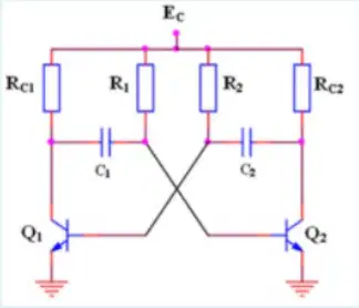
Se considera circuitul basculant astabil din imagine. Selectati afirmatiile corecte(2 raspunsuri)
a)
Circuitul se poate afla doar în stări instabile
b)
Descărcarea condensatorului C2 prin tranzistorul Q2 determina scăderea potențialului in baza tranzistorului Q1
c)
Descărcarea condensatorului C2 prin tranzistorul Q2 determina creșterea potențialului in baza tranzistorului Q1
d)
Circuitul se poate afla în două stări, una stabilă și una stabilă
53.
a)
a
b)
s
54.
a)
a
b)
c
55.

a)
s
b)
d
56.
a)
as
b)
dsd
57.
a)
dsad
b)
sdad
58.
a)
dsad
b)
asdad
59.
Pentru asigurarea unui curent mare de iesire, driverul 4511 are prevazut la iesire un: (1 raspuns)
a)
Amplificator cu reactie negativa
b)
Amplificator cu reactie pozitiva
c)
Tranzistor cu efect de camp cu canal p
d)
Tranzistor bipolar
e)
Nimic
60.
La dispozitivele de căutare hardware CAM codificatorul: (1 raspuns)
a)
Returnează datele din memorie pe baza adresei
b)
Primește datele căutate și generează adresa datelor
c)
Primește semnalele de la liniile match și generează adresa datelor căutate
d)
Returnează semnale de matching ce descriu datele căutate
61.
Selectati ordinea corecta a activarii intrarilor pentru scrierea in memoriile RAM(alegeti 1 raspuns)
a)
Adresa, selectie, semal read/write, date
b)
Adresa, semnal read/write, selectie, date
c)
Selectie, adresa, semnal read/write, date
d)
Date, adresa, selectie, semnal read/write
62.
La un tranzistor MOS la care nu aplicam potential in grila: (1 raspuns)
a)
Daca intre drena si sursa se aplica o tensiune pozitiva, una din jonctiuni este polarizata invers => nu exista curent intre drena si sursa => tranzistorul este blocat
b)
Daca intre drena si sursa se aplica o tensiune pozitiva, una din jonctiuni este polarizata invers => nu exista curent intre drena si sursa => tranzistorul functioneaza in regim normal
c)
Daca intre drena si sursa se aplica o tensiune pozitiva, una din jonctiuni este polarizata invers => nu exista curent intre drena si sursa => tranzistorul functioneaza in regim invers
63.
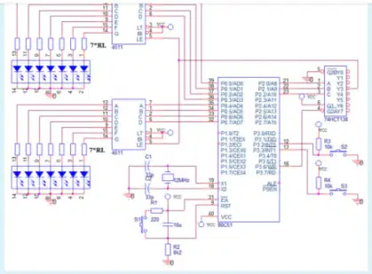
Se considera sistemul cu microcontroller 80C51 din figura. Care afirmatii sunt adevarate? (4 raspunsuri)
a)
b. Stim ca pentru lo4-10mA, circuitul 4511 are Voyo -4,25V. Pentru ca Vico-2V si lucb=10mA, valoarea aproximativa a rezistentei RL prin care este comandat LED-ul va fi de 2250 c. Pentru scrierea portului de iesire se foloseste selectia totala
b)
e. Sistemul are un port de iesire care poate fi scris prin intermediul unei variabile localizata la adresa 7B02H
c)
i. Pentru scrierea portului de iesire se foloseste selectia partiala
d)
j. Circuitul de reset asigura la intrarea in microcontroller un nivel logic O daca tasta nu este apasata
e)
a. Pentru scrierea portului de iesire se foloseste selectia liniara
64.
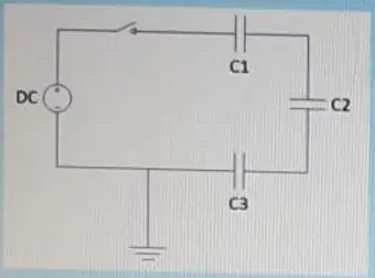
Bifati varianta corecta, considerand circuitul de mai jos: (1 raspuns)
a)
Tensiunile pe cei trei condensatori vor fi intotdeauna egale
b)
Capacitatea electrica pe intreg circuitul e data de suma capacitatilor condensatorilor
c)
Tensiunea masurata pe un condensator poate sa fie cel mult egala cu tensiunea sursei
d)
Pentru o buna functionare a circuitului, nu este necesar un alt element de circuit pe langa cei trei condensatori
65.
Bifati varianta gresita referitoare la semnalele electrice: (1 raspuns)
a)
Cu cat creste perioada unui semnal sinusoidal, cu atat scade pulsatia
b)
Semnalele electrice unidimensionale pot fi doar continue
c)
Inversul frecventei reprezinta perioada
d)
Amplitudinea semnalului este o caracteristica atat pentru semnalele digitale cat si pentru cele analogice
66.
Despre nivelurile logice ale portii fundamentale SI-NU construita in tehnologie TTL, se pot afirma urmatoarele: (2 raspunsuri)
a)
Pentru a genera "1" logic, tensiunea minim acceptata la iesire este de 2V
b)
Pentru a fi comandata cu "1" logic, tensiunea minima acceptata la intrare este 2,4V
c)
Tensiunea maxim acceptata la iesire pentru a genera "0" logic este de doua ori mai mare decat tensiunea maxim acceptata la intrare pentru a fi comandata cu "0" logic
d)
Tensiunea minim acceptata la iesire pentru a genera "1" logic este mai mare decat tensiunea minim acceptata la intrare pentru a fi comandata cu "1" logic
e)
Tensiunea la care tensiunile de intrare si de iesire sunt egale se numeste tensiune prag
67.
a)
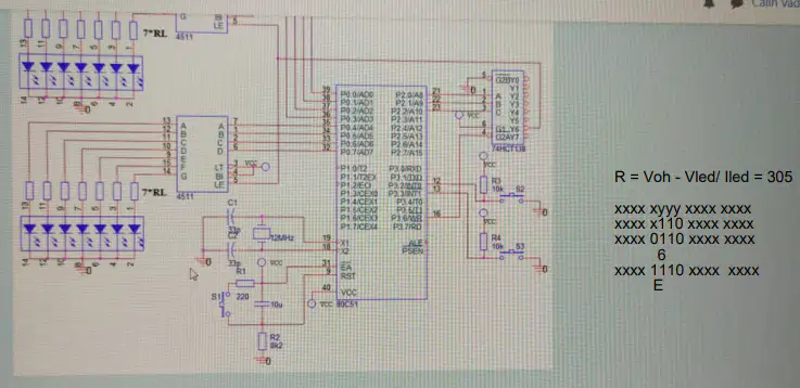
a. Pentru scrierea portului de iesire se foloseste selectia partiala
b)
b. Stim ca pentru loн=10mA, circuitul 4511 are Voнtyp 4,25V. Pentru ca VLED=1,2V SI ILED=10mA valoarea aproximativa a rezistentei RL prin care este comandat LED-ul va fi de 3050
c)
C. Circuitul de reset nu filtreaza salturile de tensiune la apasarea tastei
d)
d. Circuitul de reset filtreaza salturile de tensiune la apasarea tastei
e)
e. Stim ca pentru loн=10mA, circuitul 4511 are VoHtyp=4,25V. Pentru ca VLED=1,2V SI ILED=10mA, valoarea aproximativa a rezistentei RL prin care este comandat LED-ul va fi de 105 ohm
68.
Choose the correct answer variants for CMOS logic circuits(2 answers)
a)
Posibility that in static regime the number of driven loads to be very high
b)
Extremely low power consumption
c)
Output signal levels extremely close to the power supply voltage value for logic state 0
d)
Narrow operating temperature range
e)
Output signal levels extremely close to 0 V for logic state 1
69.
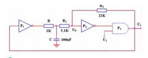
Select the correct statement about the Trigger-Schmidt controlled oscillator from the picture: (1 answer)
a)
If the control signal Ui has the value of logical 1, the circuit will behave as an oscillator
b)
dsd
70.
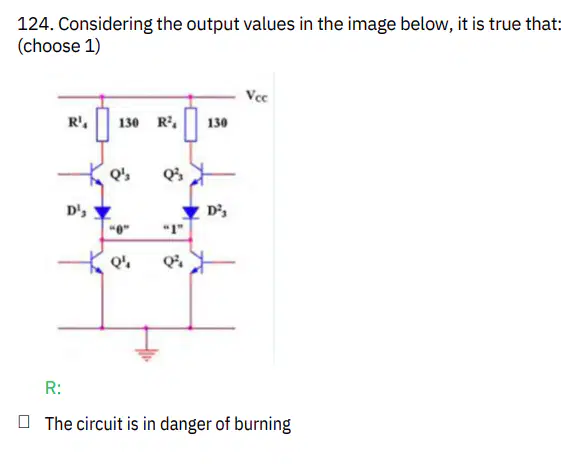
a)
das
b)
dsa
71.

Pentru circuitul de mai jos, calculati căderile de tensiune și curenții prin rezistori: (alegeți 1 răspuns)
a)
a. UR1=5V, I1≈ 1mA UR2=15V, I2≈ 2.5mA UR3≈ 5V, 13≈ 1mA
b)
b. UR1=10V, I1 = 1.5mA UR2 10V, I2≈ 1.2mA UR3=10V, 13≈ 2.5mA
c)
c. UR1≈ 6V, I1≈ 1.25mA UR2≈10V, I2≈0.75A UR3 4.5V, 13 3.2mA
d)
d. UR1=10V, I1=1.66mA UR2≈10V, I2≈1mA UR3≈ 10V, 13≈ 2mA
72.
Semiconductor diode-at thermal equilibrium:(1 answer)
a)
The electric current will best pass through the semiconductor
b)
The semiconductor acts as a low value resistor
c)
Electric current will not be produced at all through the semiconductor
d)
The electric current will partially pass through the semiconductor
73.
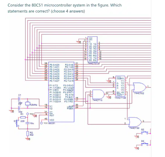
Consider the 80C51 microcontroller system in the figure. Which statements are correct?(4 answers)
a)
The clock generator circuit consists of both external components of the microcontroller and components integrated in it
b)
The system has an input port that can be read through a variable located at adress C237H
c)
The partial selection is used to activate the input port
d)
The system has an output port that can be written through a variable located at adress 41B7H
e)
The linear selection is used to activate the input port
74.

Stabilizator cu reactie cu amplificator de eroare: (2 raspunsuri)
a)
Circuitul stabilizeaza tensiunea chiar daca RL isi modifica valoarea
b)
Circuitul isi stabilizeaza tensiunea doar daca RL nu isi modifica valoarea
c)
Stabilizarea este obtinuta prin reactie pozitiva
d)
Stabilizarea este obtinuta prin reactie negativa
75.
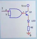
Circuitul din figură folosește o poarta CMOS pentru a comanda un LED. Alegeți valoarea aproximativă a rezistenței RE ştiind că Vcc, care alimentează şi circuitul integrat, este de 5V. Pentru LED se consideră următoarele valori: VLED=1,35V şi ILED=20mA. (alegeţi 1 răspuns)
a)
120
b)
50
c)
1,6k
d)
170
e)
1k
76.
Care dintre urmatoarele reșatii sunt adevarate in cazul unui tranzistor bipolar aflat in regiunea activa normala?(2 rapsunsuri)
a)
Ic=Ie+Ib
b)
Ic=beta*Ib
c)
Vbe=0,2V
d)
Ib=beta*Ie
e)
Ie=Ic+Ib
77.

In imaginea de mai jos, ce valor logice trebuie aplicate pe intrarile A si B pentru a obtine la iesire "0" logic?(1 raspuns)
a)
A=1, B=1
b)
A=1, B=0
c)
A=0, B=1
d)
A=0, B=0
78.
Care dintre următoarele relaţii sunt adevărate în cazul unui tranzistor bipolar aflat în regiunea de saturație? (2 raspunsuri)
a)
a. Vbe ≈ 0,75V
b)
b. le = Ic + lb
c)
c. lc = le + lb
d)
d. Ic > beta * Ib
e)
e. Vbe ≈ 0,2V
79.
Care este rolul caracteristicii de histerezis? (1 raspuns)
a)
mentine nivelul 1 logic la output indiferent de input
b)
defineste niveluri diferite la intrare pentru trecerea intre starile de 0 si 1 logic pentru a nu reactiona la variatii mici de tensiune
c)
mentine nivelul 0 logic la output indiferent de input
d)
se asigura ca trecerea intre starile 0 si 1 logic are loc la aceeasi tensiune de prag
80.
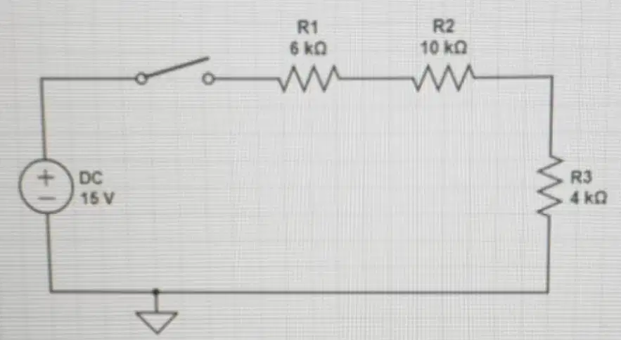
Pentru circitul de mai jos, calculati caderile de tensiune si curentii prin rezistori: (1 raspuns)
a)
a. UR1 ≈ 4.5V, I1 ≈ 0.75mA, UR2 ≈ 7.5V, I2 ≈ 0.75mA, UR3 ≈ 3V, I3 ≈ 0.75mA
b)
b. UR1 ≈ 5V, I1 ≈ 1.25mA, UR2 ≈ 8V, I2 ≈ 1.25A, UR3 ≈ 2V, I3 ≈ 1.25mA
c)
c. UR1 ≈ 5V, I1 ≈ 0.5mA, UR2 ≈ 5V, I2 ≈ 0.75mA, UR3 ≈ 5V, I3 ≈ 1.5mA
d)
d. UR1 ≈ 3V, I1 ≈ 1mA, UR2 ≈ 9V, I2 ≈ 1mA, UR3 ≈ 3V, I3 ≈ 1mA
81.
Despre timpii de propagare in circuitele logice integrate, se pot afirma urmatoarele: (2 raspunsuri)
a)
a. Timpii de intarziere se calculeaza exclusiv pe baza semnalului de iesire;
b)
b. Timpii de crestere si de cadere (Rise Time si Fall Time) se definesc pentru fronturile de tensiune ale semnalului;
c)
c. Timpul de propagare nu influenteaza valoarea maxima a frecventei semnalului de intrare;
d)
d. Timpul de propagare mediu nu include timpii de intarziere;
e)
e. Se definesc tinand cont de amplitudinea semnalului de intrare, precum si a celui de iesire
82.
Intr-o sursa de tensiune continua, transformatorul... (2 raspunsuri)
a)
a. modifica in secundar o forma de unda din primar
b)
b. genereaza o tensiune cat mai apropiata de tensiunea continua
c)
c. atenueaza variatiile de tensiune furnizate de redresor
d)
d. poate scadea sau creste in secundar valoarea tensiunii din primar
e)
e. separa aparatul de reteaua de curent alternativ
83.
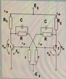
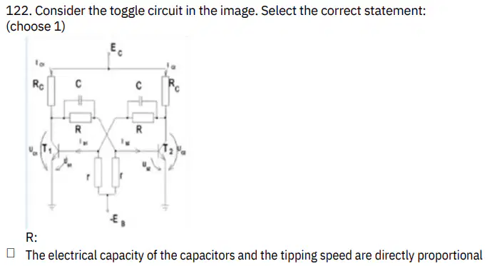
Se considera circuitul basculant din imagine. Selectati afirmatia corecta: (1 raspuns)
a)
a. Cricuitul functioneaza ca un bistabil cand rezistenta are valoarea 0
b)
b. Rezistenta r este dimensionata pentru a avea doar tensiune negativa in baza tranzistorilor T1 si T2.
c)
c. Rezistenta r nu poate avea valoarea 0 pentru ca circuitul sa poata functiona ca un bistabil
d)
d. Cresterea tensiunii in Uc2 va fi transmisa in baza tranzistorului T1 daca rezistenta r are valoarea 0
84.
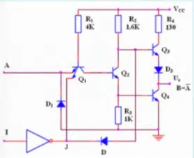
In imaginea de mai jos, ce valori trebuie aplicate intrarilor A si I pentru ca tranzistorul Q1 sa se afle in regiunea activa inversa: (1 raspuns)
a)
a. A = 0V, I = 5V
b)
b. A = 0V, I = 0V
c)
c. A = 5V, I = 5V
d)
d. A = 5V, I = 0V
85.
La memoriile CAM semnalele de matching (1 raspuns):
a)
a. Sunt preincarcate la '0' logic
b)
b. Starea '1' logic indica faptul ca exista cel putin un bit memorat care nu corespunde cu bitul cautat
c)
c. Starea '0' logic indica faptul ca exista cel putin un bit memorat care nu corespunde cu bitul cautat
d)
d. Sunt preincarcate la '1' logic
86.
Selectati ordinea corecta de executie a etapelor executate de un microcontroller pentru gestionarea unei intreruperi (1 raspuns):
a)
a. Determina sursa de intrerupere, acceseaza tabela vectorilor de intrerupere, executa rutina de tratare a intreruperii, salveaza pe stiva locatia urmatoarei instructiuni, incarca de pe stiva locatia urmatoarei instructiuni
b)
b. Determina sursa de intrerupere, executa rutina de tratare a intreruperii, acceseaza tabela vectorilor de intrerupere, salveaza pe stiva locatia urmatoarei instructiuni, incarca de pe stiva locatia urmatoarei instructiuni
c)
c. Determina sursa de intrerupere, salveaza pe stiva locatia urmatoarei instructiuni, incarca de pe stiva locatia urmatoarei instructiuni, acceseaza tabela vectorilor de intrerupere, executa rutina de tratare a intreruperii
d)
d. Salveaza pe stiva locatia urmatoarei instructiuni, determina sursa de intrerupere, acceseaza tabela vectorilor de intrerupere, executa rutina de tratare a intreruperii, incarca de pe stiva locatia urmatoarei instructiuni
87.
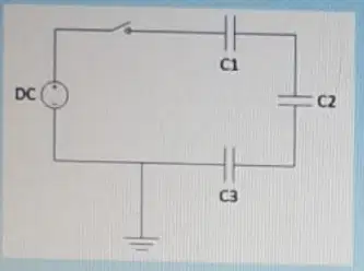
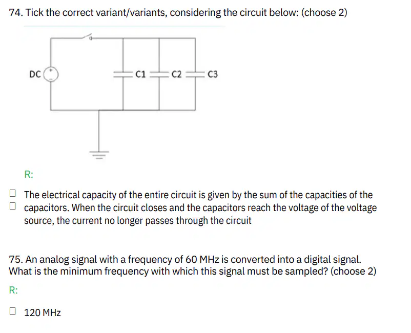
Bifati varianta corecta, considerand circuitul de mai jos: (1 raspuns)
a)
Tensiunile pe cei trei condensatori vor fi intotdeauna egale
b)
Capacitatea electrica pe intreg circuitul e data de suma capacitatilor condensatorului
c)
Tensiunea masurata pe un condensator poate sa fie cel mult egala cu tensiunea sursei
d)
Pentru o buna functionare a circuitului, nu este necesar un alt element de circuit pe langa cei trei condensatori
88.
Bifati varianta gresita referitoare la semnalele electrice: (1 raspuns)
a)
Cu cat creste perioada unui semnal sinusoidal, cu atat scade pulsatia
b)
Semnalele electrice unidimensionale pot fi doar continue
c)
Inversul frecventei reprezinta perioada
d)
Amplitudinea semnalului este o caracteristica atat pentru semnalele digitale, cat si pentru cele analogice
89.
Despre nivelurile logice are portii fundamentale Si-NU construita in tehnologie TTL, se pot afirma următoarele: (2 raspunsuri)
a)
Pentru a genera '1' logic, tensiunea minim acceptata la iesire este de 2V
b)
Pentru a fi comandata cu '1' logic, tensiunea minim acceptata la intrare este 2,4V
c)
Tensiunea maxim acceptata la iesire pentru a genera '0' logic este de doua ori mai mare decar tensiunea maxim acceptata la intrare pentru a fi comandata cu '0' logic
d)
Tensiunea minim acceptata la iesire pentru a genera '1' logic este mai mare decat tensiunea minim acceptata la intrare pentru a fi comandata cu '1' logic
e)
Tensiunea la care tensiunile de intrare si iesire sunt egale se numeste tensiune de prag
90.
Factorul de calitate al circuitelor logice reprezinta...(1 raspuns)
a)
Suma dintre timpii de propagare
b)
Diferenta in modul dintre consumul de putere in regim static si dinamic
c)
Raportul dintre consumul de putere si timpul de propagare
d)
Produsul dintre timpul de propagare si consumul de putere
91.
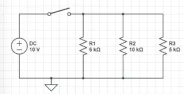
Pentru circuitul de mai jos, calculati caderile de tensiune si curentii prin rezistori: (1 raspuns)
a)
UR1 ≈ 5V, I1 ≈ 1mA, UR2 ≈ 15V, I2 ≈ 2.5mA, UR3 ≈ 5V, I3 ≈ 1mA
b)
UR1 ≈ 10V, I1 ≈ 1.5mA, UR2 ≈ 10V, I2 ≈ 1.2mA, UR3 ≈ 10V, I3 ≈ 2.5mA
c)
UR1 ≈ 6V, I1 ≈ 1.25mA, UR2 ≈ 10V, I2 ≈ 0.75mA, UR3 ≈ 4.5V, I3 ≈ 3.2mA
d)
UR1 ≈ 10V, I1 ≈ 1.66mA, UR2 ≈ 10V, I2 ≈ 2mA, UR3 ≈ 10V, I3 ≈ 2mA
92.
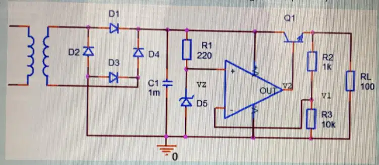
Stabilizator cu reactie cu amplificator de eroare: (2 raspunsuri)
a)
Circuitul stabilizeaza tensiunea chiar daca RL isi modifica valoarea
b)
Circuitul stabilizeaza tensiunea doar daca RL nu isi modifica valoarea
c)
Stabilizarea este obtinuta prin reactie pozitiva
d)
Stabilizarea este obtinuta prin reactie negativa
93.
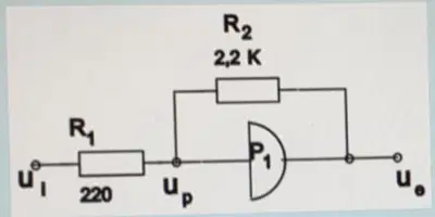
Considerand circuitul Trigger-Schmitt din imagine, selectati afirmatiile corecte: (1 raspuns)
a)
Up are tot timpul o valoare mai mare decat Ue
b)
Dupa tranzitia portii P1 din 0 -> 1 logic, diferenta dintre Ue si Up va creste pe masura ce creste Ui
c)
Dupa tranzitia portii P1 din 0 -> 1 logic, diferenta dintre Ue si Up va scadea pe masura ce creste Ui
d)
Dupa tranzitia portii P1 din 0 -> 1 logic, Ue va avea o valoare egala cu Up
94.
a)
Option 1
b)
Option eleven
95.
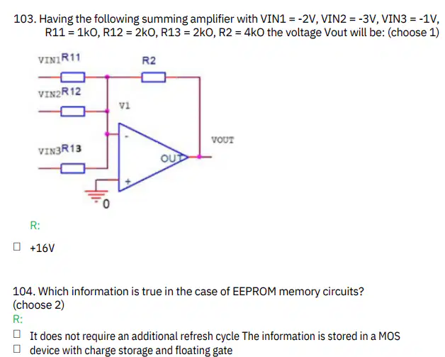
a)
Option 1
b)
Option 2
96.
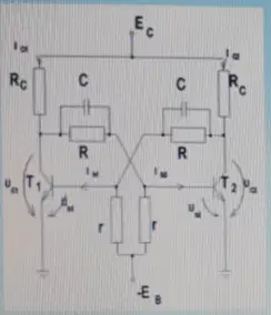
Se considera circuitul basculant din imagine. Selectati afirmatiile corecte: (2 raspunsuri)
a)
Bucla de reactie formata din tranzistorii T1 si T2 nu este niciodata intrerupta
b)
Cresterea tensiunii in baza tranzistorului T1 duce la reducerea tensiunii in baza tranzistorului T2
c)
Ambii tranzistori T1 si T2 se pot afla simultan in starea de saturatie
d)
Divizorul rezistiv R-r transmite cresterea Uc2 in baza tranzistorului T1
e)
Cresterea curentului Ic1 duce la cresterea tensiunii Uc1
97.
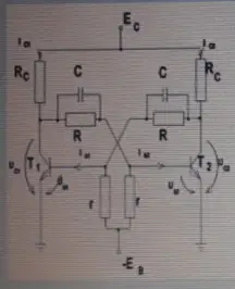
Se considera circuitul basculant din imagine. Selectati afirmatia corecta: (1 raspuns)
a)
Capacitatea electrica a condensatorului nu influenteaza vitea de basculare
b)
Condensatorii incetinesc procesul de amplificare pentru a nu se supraincalzi circuitul
c)
Capacitatea electrica a condensatorilor si viteza de basculare sunt directe proportionale
d)
Pentru a duce tranzistorii in starile T1 = saturat si T2 = blocat, amplificarea din bucla de reactie trebuie sa fie subunitara
98.
Despre factorul de incarcare al portii fundamentale SI-NU construita in tehnologie TTL, se pot afirma urmatorele: (2 raspunsuri)
a)
Factorul de incarcare la iesire pentru nivelul '0' logic este de doua ori mai mic decat factorul de incarcare la iesire pentri nivelul '1' logic
b)
Valoarea factorului de incarcare la iesire reprezinta numarul minim de porti care pot fi comandate de poarta SI-NU
c)
Factorul de incarcare la iesire pentru nivelul '0' logic este mai mic ca 1
d)
Factorul de incarcare la iesire se calculeaza pe baza curentilor de iesire ai portii care comanda si a curentilor de intrare ai portilor comandate
e)
Pe baza factorului de incarcare, o poarta SI-NU implementata printr-un circuit TTL, poate comanda intre 10 si 20 de porti SI-NU de acelasi fel
99.
Bifati variantele corecte referitoare la impuls: (2 raspunsuri):
a)
Pentru a defini corect perioada impulsului, aceasta trebuie sa fie mai mica decat durata regimului tranzitoriu din circuit
b)
Prin compunerea a 2 semnale de tip treapta se poate obtine un impuls
c)
Pentru a defini corect perioada impulsului, aceasta trebuie sa fie mai mare decat durata regimului tranzitoriu din circuit
d)
Timpul de ridicare a impulsului este acelasi cu timpul de coborare
100.
Pentru stocarea datelor/programului unui microcontroller se poate utiliza, din punct de vedere al componentelor hardware, fie o singura memorie ce contine si date si program, fie doua memorii separate, una pentru date, alta pentru program. Care sunt efectele utilizarii unei singure memorii in loc de doua? (2 raspunsuri)
a)
Reducerea dimensiunii circuitului final
b)
Cresterea consumului de putere al circuitului
c)
Cost mai redus al componentelor
d)
Necesitatea utilizarii a doua magistrale separate pentru accesul la memorie
101.
Care dintre afirmatiile legate de consumul de putere in circuitele logice integrate sunt false? (2 raspunsuri)
a)
Puterea consumata in regim de comutatie este direct proportionala cu frecventa de comutare a circuitului logic
b)
Curentul de iesire in scurtcircuit reprezinta un parametru caracteristic al consumului de putere
c)
Puterea consumata in regim de comutatie este direct proportionala cu patratul tensiunii de alimentare
d)
Puetera totala consumata reprezinta diferenta dintre puterea consumata in curent continuu si puterea consumata in regim de comutatie
e)
Puterea consumata in curent continuu are o valoare mai mare decat puterea consumata in regim de comutatie
102.
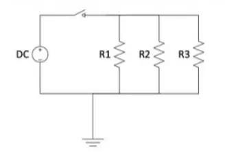
Bifati variantele corecte, considerand circuitul din figura de mai jos: (2 raspunsuri)
a)
Pentru a calcula rezistenta pe intreg circuitul, trebuie sa adunam valorile tuturor rezistorilor
b)
Diferenta de potential pe fiecare dintre rezistori e aceeasi
c)
La fiecare nod de circuit, curentul se imparte in functie de valoarea rezistorilor
d)
Oriunde am masura, curentul in circuit este acelasi
103.
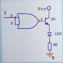
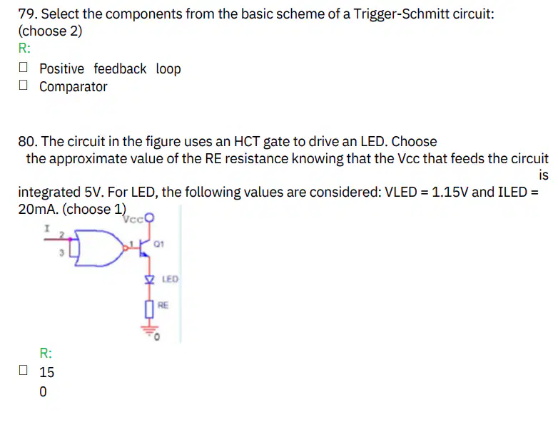
Circuitul din figura foloseste o poarta CMOS pentru a comanda un LED. Alegeti valoarea aproximativa a rezistentei RE stiind ca Vcc, care alimenteaza si circuitul integrat, este de 5V. Pentru LED se considera urmatoarele valori: VLED = 1,35V si ILED = 20mA. (1 raspuns)
a)
120
b)
50
c)
1.6k
d)
170
e)
1k
104.
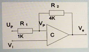
Considerand circuitul Trigger-Schmitt din imagine, care sunt factorii care determina intervalul de histerezis? (2 raspunsuri)
a)
Utilizarea unui comparator in locul unui amplificator
b)
Intrarea Vi setata la 1 logic
c)
Diferenta dintre nivelurile superioare si inferioare ale tensiunii de iesire
d)
Raportul dintre rezinstentele R1 si R2
105.
Care sunt avantaje ale folosirii tranzistoarelor MOS? (2 raspunsuri)
a)
Actiune rapida a regiunii de saturatie
b)
Densitate de integrare mai mare
c)
Folosirea ca rezistenta intre sursa si drena, rezistenta activa, faciliteaza cresterea factorului de integrare
d)
Mai usor de programat in VHDL
106.
Care afirmatii sunt adevarate in cazul circuitelor de memorie bazate pe celula de memorie SRAM CMOS? (2 raspunsuri)
a)
Operatia de citire nu este distructiva
b)
Este o memorie volatila
c)
Este o metoda adresabila prin continut
d)
Este o metoda nevolatila
e)
Operatia de citire este distructiva
107.
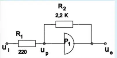
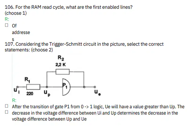
Considerand circuitul Trigger-Schmit din imagine, selectati afirmatiile corecte: (2 raspunsuri)
a)
Scaderea diferentei de tensiune dintre Ui si Up determina scaderea diferentei de tesniune dintre Up si Ue
b)
Ue are tot timpul o valoare mai mare decat Up
c)
Dupa tranziția portii P1 din 0 -> 1 logic, Ue va avea o valoare mai mare decat Up
d)
Dupa tranziția portii P1 din 0 -> 1 logic, Ue va avea o valoare mai mica decat Up
108.
Selectati care dintre urmatoarele circuite sunt CNA (convertoare numeric analogice): (2 raspunsuri)
a)
Cu aproximatii succesive
b)
Cu rezistente ponderate
c)
Cu retea de rezistente R-2R
d)
Cu simpla rampa
100 %

