
 Worksheets
Computer architechture
Total questions: 50
Worksheet time: 31mins
Explain the truth table for an OR gate.
A | B | Output, 1 | 0 | 1, 0 | 1 | 0, 1 | 1 | 0, 1 | 1 | 1
A | B | Output, 1 | 0 | 0, 0 | 1 | 0, 1 | 0 | 0, 1 | 1 | 0
A | B | Output, 0 | 0 | 0, 0 | 1 | 1, 1 | 0 | 1, 1 | 1 | 1
A | B | Output, 0 | 0 | 1, 0 | 1 | 0, 1 | 0 | 1, 1 | 1 | 0
Describe the working principle of an XOR gate.
XOR gate is a gate that outputs 1 when both inputs are 0.
XOR gate is a gate that outputs 0 when both inputs are 1.
XOR gate is a digital logic gate that gives a high output (1) only when the number of true inputs is odd.
XOR gate is a digital logic gate that gives a high output (1) only when the number of true inputs is even.
Differentiate between a half adder and a full adder.
A half adder is used for subtraction, while a full adder is used for addition.
A full adder adds two single-bit binary numbers.
A half adder adds two single-bit binary numbers, while a full adder adds three single-bit binary numbers.
A half adder adds three single-bit binary numbers.
What is the boolean operation performed by an OR gate?
Equivalent of addition
Equivalent of multiplication
Equivalent of dificsin
Equivalent of subtraction
What is the one’s complement for the binary number 011001
000111
100110
111001
110001
Which of the following gates can function on a single input?
NOT
AND
OR
NONE
What combination is a NAND gate?
NOT AND
NOT OR
NOT NOT
None of these
1. RTL stands for:
Random transfer language
Register transfer language
Arithmetic transfer language
All of these
1. Which operations are used for addition, subtraction, increment, decrement and complement function:
Bus
Memory transfer
Arithmetic operation
All of these
In which transfer the computer register are indicated in capital letters for depicting its function:
Memory transfer
Register Transfer
Bus transfer
None of these
Which operation is binary type, and are performed on bits string that is placed in register:
Logical micro operation
Arithmetic micro operation
Both
None
In every transfer, selection of register by bus is decided by:
Control signal
No signal
All signal
All of above
is a command given to a computer to perform a specified operation on some given data:
An instruction
Command
Code
None of these
If A and B are the inputs of a half adder, the carry is given by
A EXOR B
A AND B
A OR B
A XOR B
In parts of the processor, adders are used to calculate
Table Indices
Increment and Decrement Operators
Addresses
All of the Above
The Opeartion executed on data stored in registers is called
Macro-operation
Micro-Operation
Bit-Operaton
Byte-Operation
The main virtue for using single Bus structure is
Fast data transfers
Cost effective connectivity and speed
Cost effective connectivity and ease of attaching peripheral devices
None of the mentioned
In a multiplexer, the selection of a particular input line is controlled by ___________
Data controller
Selected lines
Logic gates
Both data controller and selected lines
A certain logic gate with two inputs produces a low output only when both inputs are same; then it is
an EX-OR gate
an OR gate
a NAND gate
an AND gat
The output of an AND gate will be 1 if
At least one of the inputs is at 1.
At most one of the inputs is at 0.
An even number of inputs must be at 1.
None of these.
which of the following functions is referred as complementary?
NAND
NOR
OR
NOT
RAM is usually called
Logical Memory
Physical memory
Conceptual memory
Users Memory
PSW stands for
Process status word
Program status word
Program status width
process status width
The following logic building block can be used to implement any combinational logic circuit
Ex-Or gate
Encoder
Multiplexer
Decoder
The register which holds the address of the location to or from which data are to be transferred is called
Index Register
Instruction Register
Memory Address Register
Memory Data Register
The register used as a working area in CPU is
Program Counter
Instruction Register
Instruction Decoder
Accumualtor
Which of the following register is used in the control unit of the CPU to indicate the next instruction which is to be executed ?
Accumulator
Index Register
Instruction Decoder
Program Counter
The function of program counter (PC) holds
Temporary
Address for Memory
memory Operand
Address of Instruction
This register stores the address of the memory location currently being read from or written to:
PC(Program Counter)
ACC(Accumulator)
MAR(Memory Address Register)
MDR(Memory Data Register)
CIR(Current Instruction register)
Which bus is unidirectional? (Sends data only one way)
Address bus
Data bus
Control Bus
Register bus
Stop bus
A computer uses a combination of :
Chips and peripherals
Monitor and digital pixels
Hardware and software
Keyboard and mouse

Identify the gate
NAND gate
NOR gate
A universal logic gate is one which can be used to generate any logic function. Which of the following is a universal logic gate?
OR
AND
XOR
NAND

Diagram shows a logic gate.
Which of the following will function similar to the logic gate?


Which is the truth table for the AND gate?
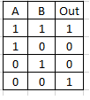
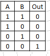
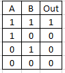
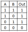
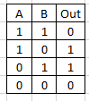
How many different combinations of 1 and 0 are possible with 3 bits?
4
5
6
7
8
a. 0
b. 1
c. 2
d. infinite
3) The boolean expression of an OR gate is _______
a) A.B
b) A’B+AB’
c) A+B
d) A’B’
4) Which of the following gate will give a 0 when both of its inputs are 1?
a) AND
b) OR
c) NAND
d) EXOR

Which Logic Gate is represented by the symbol given in the image?
a. OR
b. XNOR
c. NOR
d. XOR
A.
B.
C.
D.
What is the output of a NOR gate when both inputs are 0?
0
1
Undefined
None
What is the result of a bitwise OR operation between 10101010 and 11001100
11001100
10101010
11101110
11111111
What is the result of a bitwise AND operation between 11110000 and 11001100
11110000
11001100
11000000
00000000
Performing a bitwise XOR operation between 10101010 and 11111111 results in
01010101
B) 10101010
11111111
00000000
The bitwise operation 1010 & 1110 (using 4 bits) is equivalent to
1110
1010
1010
1000
Performing a left shift by 2 on 00001111 gives
00111100
11000000
00000011
11110000
Performing a right shift by 3 on 11110000 gives
00011110
11100000
00011100
11111000
What is the result of a circular left shift by 2 on 11001100
00110011
11001100
01100110
11110000
A circular right shift by 3 on 10000001 results in
00110000
00110001
00010000
00100000

