
 Worksheets
FINAL_SSED_Theory
Total questions: 104
Worksheet time: 52mins
If E = hc/lambda is the energy of incident photon and Eg is the energy band gap of solid state material then optical absorption will take place when
2E = Eg
E = 0
E < Eg
E >=Eg
None of the above
Luminescence is the phenomenon in which
electrons are induced to drop down to energy states
electrons are made free to accumulate at the surface
electrons are excited to high energy levels by various methods of excitation and these drop to low energy states by producing photons
holes-electrons are neutralized
A photovoltaic metal absorbs a photon of yellow light and immediately emits an ultraviolet photon. This is called
fluorescence
electroluminescence
phosphorescence.
photoluminescence
In LED, the process of emitting photons from a direct semiconductive material is called
photoluminescence
gallium arsenide
electroluminescence
gallium phosphide
The rate of direct recombination in a semiconducting material is determined by
The majority carrier lifetime, which in turn is determined by the minority carrier concentration at thermal equilibrium
The majority carrier lifetime, which in turn is determined by the majority carrier concentration at thermal equilibrium.
The minority carrier lifetime, which in turn is determined by the majority carrier concentration at thermal equilibrium.
The minority carrier lifetime, which in turn is determined by the minority carrier concentration at thermal equilibrium
GaAs is suitable for fabrication of light-emitting diodes because it is
An indirect band gap semiconductor
A direct band gap semiconductor
A wide band gap semiconductor
None of the above
Si is not suitable for fabrication of light-emitting diodes because it is:
An indirect band gap semiconductor
A direct band gap semiconductor
A wide band gap semiconductor
None of the above
Photoconductive effect means
The decreased conductivity of an illuminated semiconductor junction
The increased conductivity of an illuminated semiconductor junction
The conversion of photonic energy to electromagnetic energy
The conversion of an electromagnetic energy to photonic energy
A photoconductive cell is basically a
light emitting diode (LED)
light dependent resistor
photodiode
photoelectric relay
The resistance of an LDR __________ with increasing incident light intensity (assume that optical absorption exists).
increases
decreases
remains the same
becomes zero
None of the above
Which of the choices below is another name for a photoconductive cell?
Varicap
Varistor
Photoresistive device
Photodiode
In a semiconductor, diffusion electron current density is ___________
qDn(∂n/∂x)
qDn(∂p/∂x)
–qDp (∂p/∂x)
–qDp (∂n/∂x)
None of the above
In a semiconductor, J, Jp and Jn indicate total diffusion current density hole current density and electron
current density respectively, ∂n/∂x and ∂p/∂x are the electron and hole concentration gradient respectively in x-direction and Dp and Dn are the hole and electron diffusion constants respectively. Which one of the following equations is correct?
Jn = –qDn(∂n/∂x) for electrons
Jp = –qDp(∂p/∂x) for holes
J = –qDp (∂p/∂x) – qDn (∂n/∂x)
None of the above
The Einstein relationship between the diffusion constant Dn and mobility μn for electron is
Dn/muy n = 2kT/q
Dn/muy n = q/kT
Dn/muy n = kT/q
Dn/muy n = kT – Eg
Diffusion constant for electron is ________ to hole
Equal
Greater than
Lesser than
Can’t be determined
The continuity equation shows changes in carrier concentrations due to generation, ______, drift and diffusion
photon emission
recombination
breakdown
doping
What is the continuity equation in words?
Rate of increase = (inflow – outflow) + drift – diffusion
Rate of increase = (inflow + outflow)
Rate of increase = (inflow – outflow)
Rate of increase = (inflow – outflow) + generation – recombination
Rate of increase = (outflow + inflow) + generation – recombination
Four major steps in a planr process: i) lithography, ii) metallization, iii) ion implanation or diffusion, and iv) oxidation. Order of these steps is
i, ii, iii and iv
ii, iii, i, and iv
iii, i, ii, and iv
iv, i, iii, and ii
None of the above
The first step in a planar process of fabrication of p-n junctions is
metallization
oxidation
lithography
ion implanation or diffusion
None of the above
The second step in a planar process of fabrication of p-n junctions is
metallization
oxidation
lithography
ion implanation or diffusion
None of the above
Barrier potential in a P-N junction is caused by
Thermally generated electrons and holes
Flow of drift current.
Migration of minority carriers across the junction
Diffusion of majority carriers across the junction.
In a p-n junction, to make the depletion region extend prominently into p-region, the concentration of impurities in the p-region must be
Much less than the concentration of impurities in n-region
Much higher than the concentration of impurities in n-region
Equal to the concentration of impurities in n-region
zero
In an unbiased p-n junction, the junction current at equilibrium is
Due to diffusion of minority carriers only
Due to diffusion of majority carriers only
Zero, because equal and opposite drift and diffusion currents for electrons and holes cross the junction
Zero, because no charges cross the junction
In a step pn+ junction, WP is ____________WN
less than
much less than
greater than
much greater than
equal to
There are ______________ existed in a space charge region of an unbiased p-n junction.
electrons and holes
no electrons and holes
positive ions and electrons
no ions
In a step p +n junction, the square of the width of the depletion region is:
Directly proportional to doping in N
Inversely proportional to doping in N
Independent of doping in N
None of the above
The Fermi energy in p–n junction at thermal equilibrium is:
Proportional to distance
Directly increases with the temperature
Invariant with respect to distance
None of the above
The forward current through a semiconductor diode circuit is due to
Minority carriers
Majority carriers
Holes
Electrons
The depletion width of a pn junction _______ when the forward applied voltage increases.
increases
decreases
remains the same
becomes zero
None of the above
A silicon PN junction is forward biased with a constant current at room temperature. When the temperature is increased, the forward bias voltage across the PN junction _______________.
remains the same
increases
decreases
None of the above
When diode is in forward bias its depletion region gets
larger
narrowed
positive charges
negative charges
The depletion width of pn junction _______ when the reverse applied voltage increases
increases
decreases
remains the same
becomes zero
None of the above
When diode is in reverse bias its depletion region gets
larger
narrowed
positive charges
negative charges
The maximum reverse voltage that can be applied before current surges is called
Reverse recovery time
Maximum junction voltage
Forward voltage
Reverse breakdown voltage
A Zener diode should have:
Heavily doped p- and n-regions
Lightly doped p- and n-regions
Narrow depletion region
Both (a) and (c)
In a Zener diode (with the tunnel breakdown mechanism)
P & N regions are lightly doped
The depletion region is wide
P & N regions are heavily doped
The junction field current is small
Zener breakdown results due to
Strong electric field across the junction
Thermal decomposition
Impact ionization
Emission of free electrons
Avalance breakdown results due to
Strong electric field across the junction
Thermal decomposition
Impact ionization
Emission of free electrons
Consider a voltage regulator diode in reverse breakdown region, breakdown voltage at temperature T1 is V1, at T2 is V2. If T2 >T1 and |V1| > |V2|, the breakdown mechanism of this diode is ________________.
thermal runaway
Zener breakdown
avalanche breakdown
punch throuh
None of the above
The time taken by the diode to operate in the reversed condition from forward conduction.
Maximum power time
Reverse recovery time
Lifetime
Allocated time
The time it takes to turn off a forward-biased diode is called the _________________.
forward recovery time
recombination
reverse recovery time
turn-on time
Reverse recovery time of the diode is computed as the _______ of the storage time and trasition interval from the forward to reverse bias.
sum
product
quotient
difference
Capacitive effects are exhibited by PN junctions when they are
Forward biased
Reverse biased
Either forward or reverse biased
Neither forward nor reverse biased
What is the type of capacitance effect exhibited by the PN junction, when it is reverse biased?
Transition capacitance
Diffusion capacitance
Space charge capacitance
Drift capacitance
What is the type of capacitance effect exhibited by the PN junction when it is forward biased?
Diffusion capacitance
Storage capacitance
Drift capacitance
Transition capacitance
Diffusion or storage capacitance is the term used to refer to
the reverse bias capacitance of a diode
the forward bias capacitance of a diode
the breakdown capacitance of a zener diode
the effective capacitance of a rectifier
The variable capacitance property possessed by the reverse biased PN junction is used to construct a device known as
Zener diode
Varicap
photodiode
Tunnel diode
The sum of the resistance of the neutral p-region and the neutral n-region is called
Junction resistance
Extrinsic resistance
Intrinsic resistance
Bulk resistance
The depletion capacitance, Cj of an abrupt p–n junction with constant doping on either side varies with reverse bias, VR, as:
Cj ~ VR ^3
Cj ~ VR ^–2
Cj ~ VR^ –1/2
None of the above
The normal operating region for a zener diode is the ____________.
forward-bias region
reverse-bias region
zero-crossing region
reverse-breakdown region
Identify the false statement with respect to the Zener diode
Zener diode is needed for voltage regulation
Zener diode is operated in reverse biased condition
Zener diode has similar characteristics to that of an ideal current source
None of the above
A Schottky diode has __________.
Insulator-Semiconductor junction
Semiconductor-Semiconductor junction
Metal-Metal junction
Metal - Semiconductor junction
Schottky diodes are also known as __________.
PIN diodes
hot carrier diodes.
step-recovery diodes
tunnel diodes
The switching speed of a Schottky diode is __________
Lower than p-n junction diode
Same as p-n junction diode
Higher than p-n junction diode
None of the above
The varactor diode is:
Voltage-dependent resistance
Voltage-dependent capacitance
Voltage-dependent inductor
None of the above
In a reverse-biased photodiode with increase in incident light intensity, the diode current _________
Increases
Remains constant
Decreases
None of the above
When a photodiode is reverse biased, and kept in a dark room, the current flowing through the device corresponds to
Zero current
Maximum current the device can hold
Normal current that flows through the device
Reverse saturation current
A photodiode is used in reverse bias because
Majority of electron-hole pairs swept are reversed across the junction
Only one side is illuminated
Reverse current is small compared to photocurrent
Reverse current is large compared to photocurrent
The color emitted by an LED depends mainly on
Type of material used
Type of biasing applied
Recombination rate of charge carriers
Environmental conditions
A MOSFET is sometimes called ____________
MESFET
JFET
IGFET
SCR
None of the above
A MOSFET is sometimes called ____________.
MISFET
JFET
MESFET
SCR
None of the above
A MOSFET is sometimes called _____FET
Open gate
Shorted gate
Metallic gate
Insulated gate
A ________ is considered a voltage controlled device
FET
Diode
BJT
Capacitor
An N-EMOS will have a collection of holes under the gate oxide during
accumulation
depletion
inversion
all of the above
An N-EMOS will have a collection of electrons under the gate oxide during
accumulation
depletion
inversion
all of the above
A MOS capacitor of an N-EMOS is in the accumulation mode. The dominant charge in the channel is due to the presence of
holes
electrons
positively charged icons
negatively charged ions
Which of the following does not affect the threshold voltage of an MOSFET?
Fermi potential
gate-semiconductor work function
drain-to-source voltage
impurities implanted into the channel
The condition for MOS capacitor (N-EMOS) in depletion is
VGS < VFB
VFB < VGS < VTN
VGS > VTN
VGS = 0 V
None of the above
For an N-EMOS, Source and Drain regions are made with ______
n-type semiconductor
p-type semiconductor
intrinsic semiconductor
Metal
For an N-EMOS, substrate (or body) region are made with ______.
n-type semiconductor
p-type semiconductor
intrinsic semiconductor
Metal
For an N-EMOS, the region between Source and Drain regions is ________ region when VGS < VTN
depletion
inversion
breakdown
Ohmic
None of the above
For an N-EMOS, there is the ______ channel between Source and Drain when VGS > VTN.
resistance
water
electron
hole
None of the above
In an N-EMOS, the polarity of the inversion layer is the same as that of the
polarity of the gate electrode
minority carriers in the drain
majority carries in the substrate
majority carries in the source
An N-EMOS is in saturation mode, if VDS increases then the effiective channel length ________.
unchanges
increases
increases a half
decreases
None of the above
A MOSFET is called short-channel MOSFET when its channel length L ______
> 1 micro m
< 1 micro m
= 1 micro m
= 0.5 micro m
None of the above
An N-EMOS is in saturation mode and VDS=const, if channel length L decreases then ID________.
unchanges
increases
increases a half
decreases
None of the above
An N-EMOS is in saturation mode and VDS=const, if gate width W decreases then ID________.
unchanges
increases
increases a half
decreases
None of the above
For an N-EMOS in the saturation mode, the drain current ID
Decreases with increases in VDS
Decreases with decrease in VDS
Increases with increases in VGS
Increases with decrease in VGS
For an N-EMOS with a constant gate-source voltage (VGS > VTN), if the drain-source voltage is increased (more positive) pinch-off would occur for:
high values of drain current
saturation value of drain current
zero drain current
gate current equal to drain current
For an N-EMOS in the pinch-off region as the drain voltage is increased the drain current ___________
becomes zero
abruptly decreases
abruptly increases
remains constant
For small values of drain to source voltage, N-EMOS behaves like a (assume VGS > VTN)
Diode
Capacitor
Inverter
Resistor
An N-EMOS operates as an electronic switch, if MOSFET is in _______ region, then this switch is ON
triode
saturation
cut-off
brerakdown
4 ĐS trên đều sai
When the drain current ID is plotted against the drain-source base voltage VDS at constant gate-source voltage VGS, this curve is called ___________.
output characteristic curve
input characteristic curve
transfer characteristic curve
linear curve
When the drain current ID is plotted against the gate-source base voltage VGS at constant drain-source voltage VDS, this curve is called ___________.
output characteristic curve
input characteristic curve
transfer characteristic curve
linear curve
On the output characteristic curve of an N-EMOS for VGS > VTN, the pinch-off voltage (VDSsat) is
VGS + VTN
VGS – VTN
–VGS + VTN
–VGS – VTN
None of the above
The drain current of N-EMOS in saturation is given by ID = K(VGS – VTN) 2 where K is a constant. The magnitude of the transconductance gm is ________.
K(VGS – VTN)^2 /VDS
2K(VGS – VTN)
ID/(VGS – VDS)
K(VGS – VTN)^2 /VGS
A BJT has
One PN junction
Two PN junctions
Three PN junctions
Four PN junctions
For a typical transistor, which one of the following statements is correct?
The current IB is approximately equal to the current IE
The current IB is approximately equal to the current IC
The current IC is approximately equal to the current IE.
The sum of the current IC and IE is approximately equal to the current IB.
A _________ is considered a current controlled device.
Diode
FET
BJT
Resistor
In a BJT the region that is very lightly doped and is very thin is
Emitter
Base
Collector
None of these
Most of the electrons in the base of an NPN transistor flow:
out of the base lead
into the collector
into the emitter
into the base supply
In a BJT, collector current is controlled by:
collector voltage
base current
collector resistance
all of the above
In a uniformly doped BJT, assume that NE, NB and NC are the emitter, base and collector doping in atoms/cm3, respectively. If the emitter injection efficiency of the BJT is close unity, which one of the following condition is TRUE
NE = NB = NC
NE >> NB and NE > NC
NE = NB and NB < NC
NE < NB < NC
The emitter of the transistor is generally doped the heaviest because it
has to dissipate maximum power
has to supply the charge carriers
is the first region of transistor
must possess low resistance
For a BJT under saturation condition
IC = βIB
IC > βIB
IC < βIB
IC is independent of all other parameters.
When the emitter junction JE is forward biased while the collector junction JC is reverse biased, the transistor is at ________ region.
cut-off
saturation
[forward] active
breakdown
The most commonly used configuration of an npn BJT as a switch is
Common collector
Common emitter
Common base
Both common base and common collector
The ratio of which two currents is represented by α?
IC and IE
IC and IB
IE and IB
None of the above
The ratio of which two currents is represented by β?
IC and IE
IC and IB
IE and IB
None of the above
If α and β are the current gains in the CB and CE configurations respectively of a BJT, then (β – α)/αβ =
∞
1
2
0.5
None of the above
Consider an N-EMOS in saturation, if the temperature increases, then ID ________.
decreases
decreases by
half
increases
increases a little
None of the above
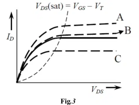
Which effect leads to curve A?
Short-channel effect.
Narrow-channel effect.
Channel-length modulation.
None of the above
Which effect leads to curve B?
Short-channel effect.
Narrow-channel effect.
Channel-length modulation.
None of the above
Which effect leads to curve C?
Short-channel effect.
Narrow-channel effect.
Channel-length modulation.
None of the above

