
Font size
 Worksheets
Ch-14 Semiconductors MCQ
Total questions: 83
Worksheet time: 47mins
The manifestation of band structure in solids is due to:
Heisenberg’s uncertainty principle
Pauli’s exclusion principle
Bohr’s postulates
Boltzmann’s law
The probability of electrons to be found in the conduction band of an intrinsic semiconductor at a finite temperature
Increases exponentially with increasing band gap
decreases exponentially with increasing band gap
decreases with increasing temperature
is independent of the temperature of the band gap
The energy gap is maximum in:
metals
superconductors
insulators
semiconductors
Choose the only false statement from the following:
In conductors the valence and conduction bands overlap.
Substances with energy gap of the order of 10eV are insulators.
The resistivity of a semiconductor increases with increase in temperature
The conductivity of a semiconductor increases with increase in temperature.
A diode D is connected to an external resistance 100Ω and an e.m.f. of 3.5V. If the barrier potential developed across the diode is 0.5V, the current in the circuit will be:
35mA
30mA
40mA
20mA
Pure Si at 500K has equal number of electron (nₑ) and hole (nₕ) concentration of 1.5 × 10¹⁶ m⁻³. Doping by indium increases nₕ to 4.5 × 10²² m⁻³. The doped semiconductor is of
The conductivity of a semiconductor increases with increase in temperature because:
number density of free current carriers increases
relaxation time increases
both number density of carriers and relaxation time increases
number density of current carriers increase, relaxation time decreases but effect of decrease in relaxation time is much less than increase in number density
In a semiconductor material, (1/3) of the total current is carried by the holes and the remaining is carried by the electrons. The drift speed of electrons is twice that of holes at this temperature. The ratio between the number densities of electrons and holes is
21/6
5
3/8
2
Which of the following device does not respond to the intensity of light incident on it.
LED
Solar cell
Photo diode
LDR
If a small amount of antimony is added to germanium crystal
it becomes a p-type semiconductor.
the antimony becomes an acceptor atom.
there will be more free electrons than holes in the semiconductor.
its resistance is increased.
In a semiconductor
there are no free electrons at 0 K
there are no free electrons at any temperature
the number of free electrons increases with pressure
A p-type semiconductor is
positively charged
negatively charged
uncharged
uncharged at 0K but charged at higher temperatures
The impurity atoms with which pure silicon may be doped to make it a p-type semiconductor are those of
phosphorus
boron
antimony
nitrogen
The forbidden gap for germanium is,
0.12 eV
0.72 eV
7.2 eV
None of these
The process of adding impurities to a pure semiconductor is called
Mixing
Doping
Diffusing
None of the above
Let n_h and n_e be the number of holes and conduction electrons in an extrinsic semiconductor. Then
n_h > n_e
n_h = n_e
n_h < n_e
n_h ≠ n_e
In an insulator_____
the valence band is partially filled with electrons
conduction band is partially filled with electrons
conduction band is empty and the valence band is filled with electrons
conduction band is filled with electrons and valence band is empty
A solar cell is basically a
A p-type Ge semiconductor
an illuminated n-p-n type transistor
an intrinsic silicon semiconductor
an illuminated silicon p-n junction diode
When a p-n junction diode is forward biased, the flow of current across the junction is mainly due to
drifting of charges
diffusion of charges
both drift and diffusion of charges
minority charge carriers
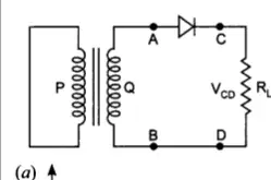
In the half-wave rectifier circuit shown. Which one of the following waveforms is true for V_CD the output across C and D?
[waveform image]
[waveform image]
[waveform image]
[waveform image]
Silicon is doped with which of the following to obtain P type semiconductor?
Phosphorus
Gallium
Germanium
Bismuth
What happens to resistance of an intrinsic semiconductor when heated?
increases
remains constant
decreases
decreases linearly
In an n-type silicon, which of the following statement is true:
Electrons are majority carriers and trivalent atoms are the dopants.
Electrons are minority carriers and pentavalent atoms are the dopants.
Holes are minority carriers and pentavalent atoms are the dopants.
Holes are majority carriers and trivalent atoms are the dopants.
Carbon, silicon and germanium have four valence electrons each. These are characterized by valence and conduction bands separated by energy band gap respectively equal to (Eg)C, (Eg)Si and (Eg)Ge. Which of the following statements is true?
(Eg)Si < (Eg)Ge < (Eg)C
(Eg)C < (Eg)Ge < (Eg)Si
(Eg)C > (Eg)Si > (Eg)Ge
(Eg)C = (Eg)Si = (Eg)Ge
In a full wave rectifier, input ac current has a frequency ‘v’. The output frequency of current is
v/2
v
2v
None of these
The depletion layer in the P-N junction region is caused by
Drift of holes
Diffusion of charge carriers
In a PN-junction diode
The current in the reverse biased condition is generally very small
The current in the reverse biased condition is small but the forward biased current is independent of the bias voltage
The reverse biased current is strongly dependent on the applied bias voltage
The forward biased current is very small in comparison to reverse biased current μA ~
The intrinsic semiconductor becomes an insulator at
0°C
100°C
300K
0K
When a forward bias is applied to a p-n junction, it
raises the potential barrier.
reduces the majority carrier current to zero.
lowers the potential barrier.
None of the above.
An object has conductivity of 50 KSm⁻¹. It is a
Conductor
Semiconductor
Insulator
Data insufficient
GaAs is
Elemental Semiconductor
Compound Semiconductor
Organic Semiconductor
None of these
The lower band which is completely occupied by the 4N valence electrons at temperature of absolute zero is
Conduction band
Doner band
Acceptor band
Valence band
No electron in conduction band results in
Insulation
Conduction
Partial Insulation
Partial conduction
In Case of Extrinsic semiconductors-
n_e = n_h = n_i
n_e >> n_h
n_e << n_h
Both B & C
I = I_e + I_h is true for-
Semiconductors
Insulator
Conductors
It never happens
If we dope an Intrinsic semiconductor with a group 15 element it becomes
Extrinsic p-type
Remain intrinsic
Extrinsic n-type
Either A or B
A semiconductor diode has
One electrode
Two electrodes
Three electrodes
No electrode
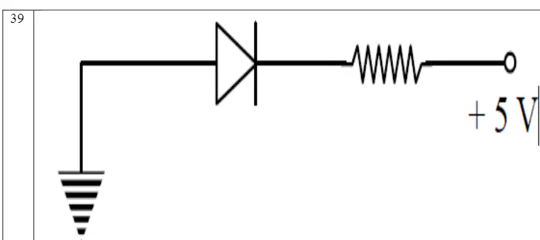
Identify the biasing
Forward
Reverse
UnBiased
Data insufficient
The reverse current shows a sudden increase at the voltage named by-
Biasing Voltage
Reverse Voltage
Breakdown Voltage
Knee Voltage
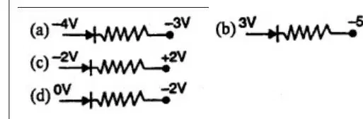
A forward biased diode is:
-4V
-3V
0V
+2V
A semiconductor device is connected in a series circuit with a battery and a resistance. A current is found to pass through the circuit. If the polarity of the battery is reversed, the current drops to almost zero. The device may be a/an
intrinsic semiconductor
p-type semiconductor
Which of the following statements is incorrect for the depletion region of a diode?
There the mobile charges exist.
Equal number of holes and electrons exist, making the region neutral.
Recombination of holes and electrons has taken place.
None of these
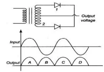
A full-wave rectifier circuit along with the input and output voltages is shown in the figure. The contribution to output voltage from diode 2 is
A, C
B, D
B, C
A, D
The cause of the potential barrier in a p-n junction diode is
depletion of positive charges near the junction
concentration of positive charges near the junction
depletion of negative charges near the junction
concentration of positive and negative charges near the junction
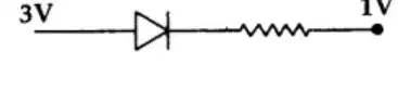
Assuming that the junction diode is ideal, the current in the arrangement shown here is:
2 mA
30 mA
20 mA
10 mA
The average value of output direct current in a full wave rectifier is
I₀/π
I₀/2
π I₀/2
2 I₀/π
An LED is constructed from a p-n junction based on a certain Ga-As-P semiconducting material whose energy gap is 1.9 eV. What is the wave length of the emitted light? (approximately):
0.620 Angstrom
0.6520 Angstrom
0.5200 nm
0.6500 nm
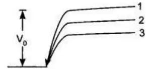
No battery is connected across the junction. In the given figure V0 is the potential barrier across a p-n junction, when
1 and 3 both correspond to forward bias of junction.
3 corresponds to forward bias of junction and 1 corresponds to reverse bias of junction.
1 corresponds to forward bias and 3 corresponds to reverse bias of junction.
3 and 1 both correspond to reverse bias of junction.
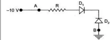
In figure given, assuming the diodes to be ideal
D1 is forward biased and D2 is reverse biased and hence current flows from A to B.
D2 is forward biased and D1 is reverse biased and hence no current flows from B to A and vice versa.
D1 and D2 are both forward biased and hence current flows from A to B.
D1 and D2 are both reverse biased and hence no current flows from A to B and vice versa.
The basic building blocks of all the electronic circuits are
Semiconductor devices require
large evacuated space
external heating arrangement
low operating voltages
high power
Which of the following statements is not correct?
With no external energy, all the valence electrons will reside in the valence band
If the lowest level in the conduction band happens to be lower than the highest level of the valence band, the electrons from the valence band can easily move into the conduction band
In insulators, electrons in the valence band all remain bound and no free electrons are available in the conduction band
Hole is created in conduction band
Electrical conductivity of a semiconductor
decreases with the rise in its temperature
increases with the rise in its temperature
does not change with the rise in its temperature
first increases and then decreases with the rise in its temperature
At absolute zero, Si acts as
metal
semiconductor
insulator
None of the above
If a small amount of arsenic is added to silicon crystal
it becomes a p-type semiconductor
it becomes an n-type semiconductor
Its resistance is increased
there will be more holes than electrons
Depletion region in a p-n junction is
a region without free electrons and holes
a region with more free electrons and holes
a region without free electrons only
a region without holes only
In forward biasing, the potential barrier across a P-N junction
increases
decreases
no change
firstly increases and then decreases
In a full wave rectifier circuit operating from 50 Hz mains frequency, the frequency in the output waveform would be
50 Hz
100 Hz
25 Hz
A pure Si crystal has 5 × 10^28 atoms m^−3. It is doped by 1 ppm concentration of pentavalent As. The number of holes is.
4.5×10⁹m−3
5.0×10⁹m−3
5×1028m−3
1.5 × 10^12 m^−3
Electric conduction in a semiconductor takes place due to
electrons only
holes only
both electrons and holes
neither electrons nor holes
The mobility of free electrons is greater than that of free holes because
they are light
they carry negative charge
they mutually collide less
they require low energy to continue their motion
When an impurity is doped into an intrinsic semiconductor, the conductivity of the semiconductor
increases
decreases
remains the same
becomes zero
An electric field is applied to a semiconductor. Let the number of charge carriers be n and the average drift speed be v. If the temperature is increased
both n and v will increase
n will increase but v will decrease
v will increase but n will decrease
both n and v will decrease
If a small amount of antimony is added to germanium crystal
it becomes a p-type semiconductor
the antimony becomes an acceptor atom
there will be more free electrons than holes in the semiconductor
its resistance is increased
A semiconductor device is connected in a series circuit with a battery and a resistance. A current is found to pass through the circuit. If the polarity of the battery is reversed, the current drops to almost zero. The device
Transistor
Diode
Resistor
Capacitor
66. may be a/an
intrinsic semiconductor
p-type semiconductor
n-type semiconductor
p-n junction diode
Diffusion current in a p-n junction is greater than the drift current in magnitude
if the junction is forward-biased
if the junction is reverse-biased
if the junction is unbiased
in no case
In a semiconductor diode, the barrier potential offers opposition to
holes in P-region only
free electrons in N-region only
majority carriers in both regions
majority as well as minority carriers in both regions
When p-n junction diode is forward biased then
both the depletion region and barrier height are reduced
the depletion region is widened and barrier height is reduced
the depletion region is reduced and barrier height is increased
Both the depletion region and barrier height are increased
In a half wave rectifier, the r.m.s. value of the a.c. component of the wave is
equal to d.c. value
more than d.c. value
less than d.c. value
zero
In Conductor, Semiconductor and Insulator, the forbidden energy gaps are E₁, E₂ and E₃ respectively. Which one is correct?
E₁
E₁>E₂=E₃
E₁=E₂
E₁>E₂>E₃
When a forward bias is applied to a p-n junction, it
raises the potential barrier.
reduces the majority carrier current to zero.
lowers the potential barrier.
None of the above.
Zener diode is fabricated by
heavily doping the p side and lightly doping the n side.
heavily doping p and n sides of the junction.
heavily doping the n side and lightly doping the p side.
lightly doping p and n sides of the junction.
The forward biased diode connection is
[diagram] 3V
[diagram] 4V
[diagram] 2V
[diagram] -2V
A P-N photodiode is fabricated from a semiconductor with a band gap of 2.5 eV. It can detect a signal of wavelength
(a)
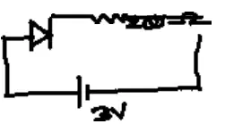
The reading of the ammeter for a silicon diode in the given circuit is
15 mA
11.5 mA
13.5 mA
0
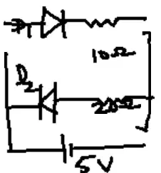
Two ideal diodes are connected to a battery as shown in Fig. Find the current supplied by the battery.
0.75 A
0.5 A
0.25 A
0
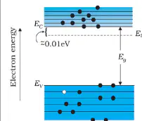
The material is a/an
p type semiconductor
n type semiconductor
insulator
metal
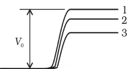
In Figure, V0 is the potential barrier across a p-n junction, when no battery is connected across the junction.
1 and 3 both correspond to forward bias of junction
3 corresponds to forward bias of junction and 1 corresponds to reverse bias of junction
1 corresponds to forward bias and 3 corresponds to reverse bias of junction.
3 and 1 both correspond to reverse bias of junction
The output from a full wave rectifier is
a pulsating unidirectional voltage
a d.c. voltage
zero
unidirectional voltage having ripples
What happens to the conductivity of a semiconductor when it is doped with a trivalent element?
It becomes an n-type semiconductor.
It becomes a p-type semiconductor.
It remains intrinsic.
It becomes an insulator.
In a semiconductor, the Fermi level is closer to the conduction band in:
p-type semiconductors
All types of semiconductors
Intrinsic semiconductors
n-type semiconductors
Which of the following statements is true regarding the temperature dependence of intrinsic semiconductors?
The conductivity decreases with increasing temperature.
The number of free electrons increases with increasing temperature.
The number of holes remains constant with temperature changes.
The number of free electrons decreases with increasing temperature.

