
 Worksheets
VLSI Design Quiz updated on 20092020
Total questions: 81
Worksheet time: 43mins
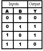
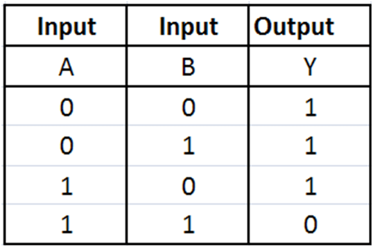
The output of an exclusive-NOR gate is 1,Which input combination is correct?
A = 1 B = 0
A = 0 B = 1
A = 0 B = 0
none of the above

VLSI technology uses ________ to form integrated circuit
transistors
switches
diodes
buffers
The CMOS gate circuit of NOT gate is


The CMOS logic circuit for NAND gate is


None of the mentioned
The CMOS logic circuit for NOR gate is


VLSI stands for
Very limited scale integration
Very large scale integration
very long scale integration
none of these
CMOS technology is used in developing
microprocessors
microcontrollers
digital logic circuits
all of the mentioned
How many terminals are there for a MOSFET
Two
Three
Four
Five
Small scale Integration circuits have
10 to 100 Transistors
100 to 1000 Transistors
1000 to 20000 Transistors
20000 to 1Million Transistors
In MOS transistors, _____ is used for their gate
Metal
Silicon di Oxide
Source/Drain
Polysilicon
All circuit components and interconnections are formed on single thin ___________(substrate) is called monolithic IC
wafer
sand
glass
non of them
The first step of IC Manufacturing is _________________
Masking
wafer production
Etching
None of them
The wafer is a round slice of ______________material such as silicon
Semiconductor
Insulator
Conductor
None of them
_________MOSFET is also called as dual MOSFET
depletion
enhancement
JFET
BJT
Transistors rely on ________, materials that are neither pure insulators nor pure conductors.
semiconductors
semi-insulators
diodes
integrated circuits
Medium scale Integration circuits have
10 to 100 Transistors
100 to 1000 Transistors
1000 to 20000 Transistors
20000 to 1Million Transistors
Large scale Integration circuits have
10 to 100 Transistors
100 to 1000 Transistors
1000 to 20000 Transistors
20000 to 1Million Transistors
Very Large scale Integration circuits have
10 to 100 Transistors
100 to 1000 Transistors
1000 to 20000 Transistors
20000 to 1Million Transistors
NMOS has N-substrate
TRUE
FALSE
PMOS has P-substrate
TRUE
FALSE
nMOS devices are formed in
p-type substrate of high doping level
n-type substrate of low doping level
p-type substrate of moderate doping level
n-type substrate of high doping level
Source and drain in nMOS device are isolated by
a single diode
two diodes
three diodes
four diodes
MOS transistors consists of
semiconductor layer
metal layer
layer of silicon dioxide
all of the mentioned
In CMOS fabrication, nMOS and pMOS are integrated in same substrate.
true
false
P-well is created on
p subtrate
n substrate
p & n substrate
none of the mentioned
The n-type semiconductor have _______ as majority carriers
Holes
Ions
electrons
positive ions
The oxide layer formed in the MOSFET is
Oxides of Non metals
Poly Silicon oxide
Silicon dioxide
Metal oxide
Which of the following terminals does not belong to the MOSFET?
Drain
Gate
Base
Source
A MOSFET has …………… terminals
4
3
5
2
__________ network to connect the output of 1
pMOS pull up
CMOS
nMOS pull down
all the above
when gate is ___________ nMOS transistor is ON
low
high
high impendence
low or high
In MOS structure for the condition Vg > Vt it will in ___________
inversion region
accumulation region
depletion region
all the above
nMOS transistor the Ids value is '0' for ______________
linear region
cutoff region
saturation region
unsaturated region
The photoresist layer is exposed to ____________
a) Visible light
b) Ultraviolet light
c) Infra red light
d) LED
The electrical equivalent component for MOS structure is:
a) Resistor
b) Capacitor
c) Inductor
d) Switch
Ids depends on ___________
a) Vg
b) Vds
c) Vdd
d) Vss
In CMOS logic circuit the n-MOS transistor acts as
Load
Pull up network
Pull down network
In CMOS logic circuit the p-MOS transistor acts as
Load
Pull up network
Pull down network
Short to ground
In CMOS logic circuit, the switching operation occurs because
Both n-MOSFET and p-MOSFET turns OFF simultaneously for input ‘0’ and turns ON simultaneously for input ‘1’
Both n-MOSFET and p-MOSFET turns ON simultaneously for input ‘0’ and turns OFF simultaneously for input ‘1’
N-MOSFET transistor turns ON, and p-MOSFET transistor turns OFF for input ‘1’ and N-MOS transistor turns OFF, and p-MOS transistor turns ON for input ‘0’
None of the mentioned
In enhancement MOSFET, the magnitude of output current __________ due to an increase in the magnitude of gate potentials.
a. Increases
b. Remains constant
c. Decreases
d. None of the above
Which type of MOSFET exhibits no current at zero gate voltage?
a. Depletion MOSFET
b. Enhancement MOSFET
c. Both a and b
d. None of the above
In MOS transistors, _____ is used for their gate
Metal
Silicon di Oxide
Source/Drain
Polysilicon
The n-MOS transistor is made up of
N-type source, n-type drain and p-type Substrate
N-type source, p-type drain and p-type Substrate
P-type source, n-type drain and n-type Substrate
P- type source, p-type drain and n-type Substrate
All circuit components and interconnections are formed on single thin ___________(substrate) is called monolithic IC
wafer
sand
glass
non of them
The first step of IC Manufacturing is _________________
Masking
wafer production
Etching
None of them
__________voltage is to be given to the gate of enhancement MOSFET to form channel and start to conduct.
Positive
Negative
any
both
The p-MOS transistor is made up of
N-type source, n-type drain and p-type Substrate
N-type source, p-type drain and p-type Substrate
P-type source, n-type drain and n-type Substrate
P- type source, p-type drain and n-type Substrate
Which among the following MOSFET type will be in ON condition when VGS = -ve volt
N - Channel Depletion
N - Channel Enhancement
P- Channel Depletion
Which among the following MOSFET type will be in ON condition when VGS = 0 volt
N-Channel Depletion
N-Channel Enhancement
P-Channel Enhancement
Which among the following MOSFET type will be in ON condition when VGS = +ve volt
N-Channel Enhancement
P-Channel Enhancement
P-Channel Depletion

Match the given transfer characteristics with the below symbol.


NMOS has N-substrate
TRUE
FALSE
PMOS has P-substrate
TRUE
FALSE
nMOS devices are formed in
p-type substrate of high doping level
n-type substrate of low doping level
p-type substrate of moderate doping level
n-type substrate of high doping level
In depletion mode, source and drain are connected by
insulating channel
conducting channel
Vdd
Vss
In enhancement mode, device is in _________ condition
conducting
non conducting
partially conducting
insulating
Enhancement mode device acts as ____ switch, depletion mode acts as _____ switch
open, closed
closed, open
open, open
close, close
______ architecture is used to design VLSI
system on a device
single open circuit
system on a chip
system on a circuit
The design flow of VLSI system is
1. Architecture design 2. Fabrication 3. System Specification 4. Circuit Design 5. Packaging and Testing 6. logic design 7. Physical Design 8. Functional Design
3-1-8-6-4-7-2-5
3-2-8-6-4-7-1-5
3-1-5-6-4-7-2-8
7-1-8-6-4-3-2-5
Electrical charge flows from
source to drain
drain to source
source to ground
source to gate
MOSFET has greatest application in digital circuit due to
Low power consumption
Less noise
Small amount of space it takes on a chip
All of the above
Ids depends on
Vg
Vds
Vdd
Vss
What is Moore's law
Number of transistors increases every 12 months
Number of transistors doubles every 18 months
Number of transistors increases every 12 months
Number of transistors triples every 18 months
An Integrated Circuit (IC) is also called as __________
FPGA
MIcrocontroller
Chip or Microchip
None of them
IC can function as _________ etc.
timer, counter
oscillator
amplifier
computer memory
All of them
Inverters are essential for ________
NAND gates
NOR gates
sequential circuits
all of the mentioned
In basic inverter circuit _____________ is connected to ground.
source
gates
drain
resistance
In inverter circuit ________ transistors is used as load
enhancement mode
depletion mode
all of the mentioned
none of the mentioned
In nMOS inverter configuration depletion mode device is called as ________
pull up
pull down
all of the mentioned
none of the mentioned
How is nMOS inverter represented?


Pass transistors are transistors used as ________
switches connected in series
switches connected in parallel
inverters used in series
inverter used in parallel
CMOS inverter has ------- regions of operation
3
4
2
5
In the region where inverter exhibits gain, the two transistors are in ------------ region
saturation
linear
cut-off
non saturation
If βn = βp, then Vin is equal to
Vdd
Vss
2Vdd
0.5Vdd
How many transistors might bring up latch up effect in p-well structure?
2
3
1
4
Substrate doping level should be decreased to avoid the latch-up effect.
true
false

