
 Worksheets
Digital & Power Electronics Class Test
Total questions: 50
Worksheet time: 24mins
What are the 3 legs of a transistor called?
Base, Electrode, Commiter
Bridge, Collector, Extruder
Base, Collector, Emitter
Brake, Collection, Emit
Transistors act like tiny "____________."
Electron sources
Switches
Batteries
Bees?

What are the names of the terminals X, Y and Z?
X = Base, Y = Collector, Z = Emitter
X = Emitter, Y = Base, Z = Collector
X = Collector, Y = Base, Z = Emitter
X = Collector, Y = Emitter, Z = Base
One function of the transistor is to_____________?
rectify
amplify
limit
control
Which terminal was heavily dopped....?
Emitter
Base
Collector
None of the above
A transistor is a …………… operated device
Voltage
Both Voltage and Current
Current
None of the Above
Amplifier circuit will be in which configuration
CE
CB
CC
None
Given that αdc = 0.980, determine
the value of βdc.
(a)
To operate properly, a transistor's base-emitter junction must be forward biased with reverse bias applied to which junction?
collector-emitter
base-collector
base-emitter
collector-base
Most of the electrons in the base of an NPN transistor flow:
out of the base lead
into the collector
into the emitter
into the base supply
In a transistor, collector current is controlled by:
collector voltage
base current
collector resistance
all of the above
A transistor has …………………
one pn junction
two pn junctions
three pn junctions
four pn junctions
The base of a transistor is ………….. doped
heavily
moderately
lightly
none of the above
A thyristor (SCR) is a
P-N-P device
N-P-N device
P-N-P-N device
P-N device
Which terminal does not belong to the SCR?
Anode
Gate
Base
Cathode
An SCR is a
four layer, four junction device
four layer, three junction device
four layer, two junction device
three layer, single junction device
In the SCR structure the gate terminal is located
near the anode terminal
near the cathode terminal
in between the anode & cathode terminal
none of the mentioned
The value of anode current required to maintain the conduction of an SCR even though the gate signal is removed is called as the
holding current
latching current
switching current
peak anode current
An SCR has three terminals viz ……………
Cathode, anode, gate
Anode, cathode, grid
Anode, cathode, drain
None of the above
SCR is a ……………….. controlled device
Voltage
Current
Voltage as well as current
None of the above
An SCR is turned off when …………..
Gate is reverse biased
Gate voltage is reduced to zero
Anode current is reduced to zero
None of the above
An SCR is a .....switch
Unidirectional
Bidirectional
THree directional
None of the above
In a SCRs
Both Latching current and holding current are associated with turn-off process
Latching current is associated with turn-off process and holding current with turn on process
Holding current is associated with turn-off process and Latching current with turn-on process
Both Latching current and holding current are associated with turn on process
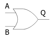
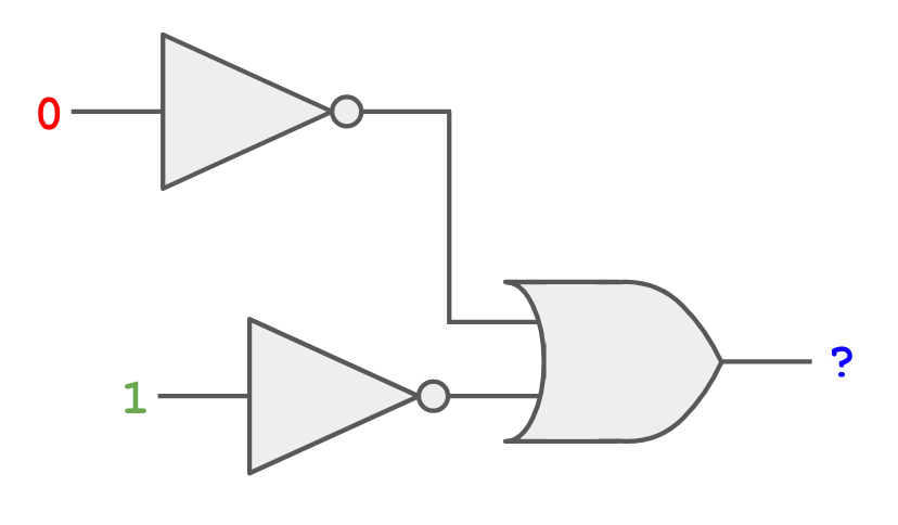
What will the circuit's output be?
1
0
Convert the binary number 01011 into decimal
10
11
13
12
Which bit has the highest weightage?
MSB
LSB
Middle most bit
none
The range of octal number is from......
1 to 8
0 to 7
0 to 9
none
The decimal equivalent of the number 101101.10 is
40.75
45.5
44.5
43.25
Full Adder can be formed by cascading two half adders
True
False
The combinational circuit used for routing the input value to the output line based on the select signal combination
Multiplexer
Demultiplexer
Encoder
Decoder
In SR Flip Flops, given the inputs S = 0, R =0, and Present state Qn = 0. Find the Next State Qn+1 .
01
1
Dont care
0
In SR flip flops , when the given inputs are S=1 and R =1 , then next state will be
No change
Reset
Indeterminant
Toggle
In S-R flip-flop, if Q = 0 the output is said to be ___________
a) Set
b) Reset
c) Previous state
The advantage of a J-K flip-flop over an S-R FF is that ________.
A.it does not require a clock input
B.it has only one output
C.it has no invalid states
In a J-K flip-flop, if J=K the resulting flip-flop is referred to as
D flip-flop
T flip-flop
S-K flip-flop
T Flip flop is used as
Transfer data circuit
Toggle switch
Time delay switch
Applications of cycloconverters include
speed control of ac drives
induction heating
static VAr compensation
all of the mentioned
The single phase bridge type cycloconverter uses __________ number of SCRs.
4
8
6
The cycloconverter require natural or forced commutation as under
Natural commutationin bothstep-up and step down cycloconverter
Forced commutation in both step-up and step-down cycloconverter
Forced commutation in step-up cycloconverter
Forced commutation in step-down cycloconverter
Materials which can conduct electricity better than insulator,but not as well as conductors. This is the definition of
diode
semiconductor
conductor
insulator
superconductor
Doping of Semiconductors
materials which can conduct electricity better than insulator, but not as well as conductors.
The process of adding of a certain amount of specific impurities atoms in the pure semiconductor.
when 4 electrons in outermost orbit.
The dv/dt protection is provided in order to
limit the power loss
reduce the junction temperature
avoid accidental turn-on of the device
avoiding sudden large voltage across the load
di/dt protection is provided to the thryistor by
connecting an inductor in parallel across the load
connecting an inductor in series with the load
connecting an inductor in parallel across the gate terminal
connecting an inductor in series with the gate

