
 Worksheets
Junior GP4 Test 1 Review
Total questions: 73
Worksheet time: 2hrs 26mins

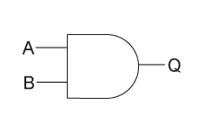


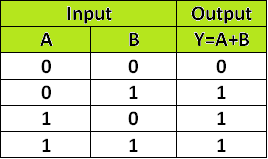
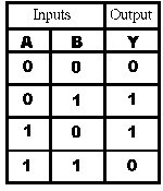
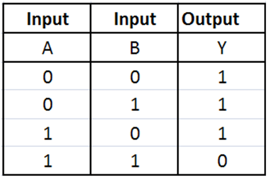
Which part of an amplifier reduces the transistor emitter current?
Emitter Resistor
Voltage Divider
Stability Capacitor
Load Resistor
Coupling Capacitor
Which part of an amplifier provides a path for unwanted AC that isn't the output?
Emitter Resistor
Voltage Divider
Stability Capacitor
Load Resistor
Coupling Capacitor
Which part of an amplifier creates a fixed bias on the base of the transistor?
Emitter Resistor
Voltage Divider
Stability Capacitor
Load Resistor
Coupling Capacitor
Which part of an amplifier changes the output signal based on the current running through the transistor?
Emitter Resistor
Voltage Divider
Stability Capacitor
Load Resistor
Coupling Capacitor
Which part of an amplifier prevents unwanted signals effecting the amplifier or leaving the amplifier?
Emitter Resistor
Voltage Divider
Stability Capacitor
Load Resistor
Coupling Capacitor
What type of signal amplifier converts a small input voltage into a much larger output voltage?
Small Signal
Large Signal
Complex Signal
Digital Signal
Analog Signal
What type of signal amplifier is designed to switch heavy load currents?
Small Signal
Large Signal
Complex Signal
Digital Signal
Analog Signal
Which amplifier configuration is most common in small signal amplifiers?
Common Emitter
Common Collector
Common Base
Common Gate
Common Source
Which amplifier configuration is most common in large signal amplifiers?
Common Emitter
Common Collector
Common Base
Common Gate
Common Source
Which amplifier configuration is the least common?
Common Emitter
Common Collector
Common Base
Common Gate
Common Source
Which classification of amplifier is the best at recreating the original signal with the least distortion?
Class A
Class B
Class AB
Class C
Which classification of amplifier only recreates half of the input signal?
Class A
Class B
Class AB
Class C
Which classification of amplifier creates the most signal distortion?
Class A
Class B
Class AB
Class C

This symbol is for
MOSFET-D type
JFET-n channel
JFET-p channel
MOSFET-E type

These symbols represent
(a) D-mode n channel MOSFET (b) D-mode p channel MOSFET
(a) D-mode n channel MOSFET (b) E-mode p channel MOSFET
(a) D-mode p channel MOSFET (b) D-mode n channel MOSFET
(a) E-mode n channel MOSFET (b) E-mode p channel MOSFET

This symbol shows
n channel E-mode MOSFET
n channel D-mode MOSFET
p channel E-mode MOSFET
p channel D-mode MOSFET
Which is true about FETs when compared to BJTs? (Select all that apply)
High output impedance
Fast switching time
Voltage Controlled
Easy to bias
Robust
Which is true about BJTs when compared to FETs? (Select all that apply)
High voltage gain
Low input impedance
Medium Noise generation
Acts like a resistor
Expensive

What are the inputs value if the output is 0
0000
0101
1111
1100
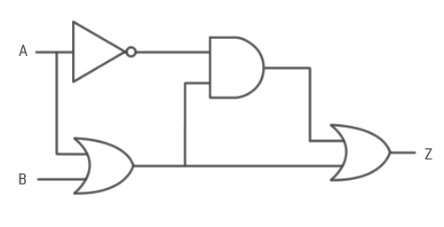
What is the output Z of this logic cricuit if A = 1 and B = 1
0
1
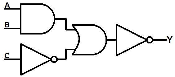
What is the output Y of this logic cricuit if A = 1, B = 1, and C = 1
0
1
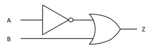
What is the Logic Expression for this circuit?
Z = NOT (A AND B)
Z = NOT (A OR B)
Z = (NOT A) AND B
Z = (NOT A) OR B
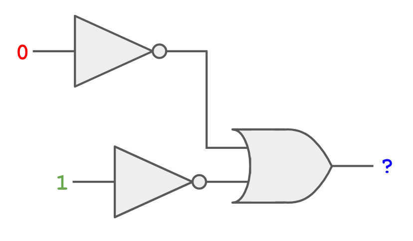
What will the circuit's output be?
1
0
What type of IC contains up to 10 to 100 transistors?
SSI
MSI
LSI
VLSI
ULSI
What type of IC contains hundreds of logic gates?
SSI
MSI
LSI
VLSI
ULSI
What type of IC would a programmable logic device be generally considered?
SSI
MSI
LSI
VLSI
ULSI
What type of IC is more commonly referred to as a System-on-Chip?
SSI
MSI
LSI
VLSI
ULSI
What series of chips are TTL based?
7400
7500
4000
5000
What series of chips are CMOS based?
7400
7500
4000
5000
For TTL, what voltage range is generally considered to be logic level LOW?
0.0 to 0.8 volts
2.0 to 5.0 volts
0.8 volts to 2.0 volts
0.0 to 1.8 volts
3.3 to 5.5 volts
For TTL, what voltage range is generally considered to be logic level HIGH?
0.0 to 0.8 volts
2.0 to 5.0 volts
0.8 volts to 2.0 volts
0.0 to 1.8 volts
3.3 to 5.5 volts
What 7400 sub-family is considered to be standard?
74Nxx
74Lxx
74ASxx
74ALSxx
74HCxx
What 7400 sub-family is considered to be low power?
74Nxx
74Lxx
74ASxx
74ALSxx
74HCxx
What 7400 sub-family is considered to have a high switching speed while utilizing Schottky diodes?
74Nxx
74Lxx
74ASxx
74ALSxx
74HCxx
What 7400 sub-family combines TTL and CMOS?
74Nxx
74Lxx
74ASxx
74ALSxx
74HCxx
Which of the following 7400 series contains Quad 2-input NAND gates?
74LS00
74L08
74AS32
74HC04
7402
Which of the following 7400 series contains Quad 2-input AND gates?
74LS00
74L08
74AS32
74HC04
7402
Which of the following 7400 series contains Quad 2-input OR gates?
74LS00
74L08
74AS32
74HC04
7402
Which of the following 7400 series contains Hex NOT gates?
74LS00
74L08
74AS32
74HC04
7402
Which of the following 7400 series contains Quad 2-input NOR gates?
74LS00
74L08
74AS32
74HC04
7402
Which transistor configuration has the lowest input impedance?
Common base
Common emitter
Common collector
Common gate
Common source
Which transistor configuration has the lowest output impedance?
Common base
Common emitter
Common collector
Common gate
Common source
Which transistor configuration has the highest voltage gain?
Common base
Common emitter
Common collector
Common gate
Common source
Which transistor configuration has the highest current gain?
Common base
Common emitter
Common collector
Common gate
Common source
Which transistor configuration has the highest power gain?
Common base
Common emitter
Common collector
Common gate
Common source
Which transistor configuration causes a 180 degree phase shift?
Common base
Common emitter
Common collector
Common gate
Common source

What transistor configuration is this?
Common Base
Common Collector
Common Emitter
Common Gate

What transistor configuration is this?
Common Base
Common Collector
Common Emitter
Common Gate

What transistor configuration is this?
Common Base
Common Collector
Common Emitter
Common Gate
If the base current of a transistor is 0.35A and the collector current is 2.47A, what is the emitter current?
(a)
If the base current of a transistor is 0.8A and the emitter current is 3.2A, what is the collector current?
(a)
On a transistor with a base current of 0.6A, collector current of 2.8A and an emitter current of 3.4A, what is the Beta current gain? (Round up to the thousandth place)
(a)
On a transistor with a base current of 0.6A, collector current of 2.8A and an emitter current of 3.4A, what is the Alpha current gain? (Round up to the thousandth place)
(a)
On a transistor with a base current of 0.6A, collector current of 2.8A and an emitter current of 3.4A, what is the Gamma current gain? (Round up to the thousandth place)
(a)
What current gain is represented by the symbol "β"?
Beta
Gamma
Alpha
Mu
What current gain is represented by the symbol "α"?
Beta
Gamma
Alpha
Mu
What current gain is represented by the symbol "γ"?
Beta
Gamma
Alpha
Mu
What is the primary current gain for common base?
Beta
Gamma
Alpha
Mu
What is the primary current gain for common collector?
Beta
Gamma
Alpha
Mu
What is the primary current gain for common emitter?
Beta
Gamma
Alpha
Mu
For an NPN transistor which pin has the highest voltage when properly biased?
Collector
Emitter
Base
Gate
For an PNP transistor which pin has the highest voltage when properly biased?
Collector
Emitter
Base
Gate

