
 Worksheets
Semiconductor and Diode Self Learning Activity 1
Total questions: 60
Worksheet time: 34mins
What is the primary characteristic of a semiconductor?
High conductivity
Low resistance to current flow
Moderate conductivity that is controllable
Very low conductivity
Which of the following is NOT a common semiconductor material?
Gallium Arsenide (GaAs)
Germanium (Ge)
Copper (Cu)
Silicon (Si)
In a P-type semiconductor, which carrier is the majority?
Produas
Neutrons
Holes
Electrons
What happens to the depletion region in a forward-biased PN junction?
It increases
It disappears completely
It decreases
It remains the same
What is the primary function of a diode?
To generate electricity
To amplify signals
To rectify current
To store energy
What is the effect of temperature on the energy gap of a semiconductor?
It increases with temperature
It decreases with temperature increase
It remains constant
It becomes infinite
What is the term for the process of adding impurities to a semiconductor?
Doping
Doping out
Rectifying
Conducting
What is the built-in potential in a PN junction?
The current flowing through the junction
The energy required to break bonds
The potential difference across the junction
The voltage drop in reverse bias
Which of the following describes the current-voltage relationship of a diode?
Non-linear
Constant
Proportional
Linear
What is the majority carrier in an N-type semiconductor?
Protons
Neutrons
Electrons
Holes
What happens to the current in a reverse-biased PN junction?
It increases significantly
It decreases to zero
It flows freely
It becomes unstable
What is the primary use of Zener diodes?
Rectification
Current limiting
Signal amplification
Voltage regulation
What is the effect of applying a forward bias to a PN junction?
It stops current flow
It narrows the depletion region
It widens the depletion region
It reverses the current flow
What is the primary purpose of a transistor?
To rectify current
To amplify signals
To store energy
To generate heat
What happens to the conductivity of a semiconductor as temperature increases?
It decreases
It remains constant
It increases
It becomes zero
Semiconductors that has been subjected to doping process and no longer pure.
(a)
The barrier voltage at a PN junction for silicon is about ………
Zero
0.5V
0.3V
0.7V
A diode is in forward biased when
For a diode, the number of minority carriers crossing the junction mainly depends on supply
Positive terminal of the battery is connected to N-side and the negative side to the P-side
Positive terminal of the battery is connected to P-side and the negative side to the N-side
N-side is connected directly to the p-side
What happens to a diode if the reverse bias voltage exceeds the breakdown voltage?
It becomes a short circuit.
It becomes an open circuit.
It continues to operate normally.
It gets damaged and stops functioning.
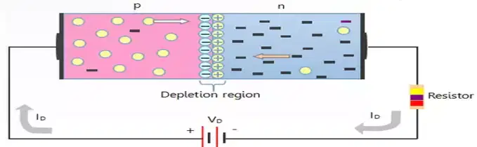
Based on figure, which statement is correct?
It decreases the current flow through the diode
It increases the current flow through the diode.
It allows the diode to conduct in the reverse direction.
It has no effect on the diode's operation.
what is the meaning of rectification?
a process of smoothing using a capacitor
a process of converting an alternating current into a direct current by using a diode.
a process of adding impurities to pure materials

The diagram is a process
of half-wave rectification
of adding impurities
of full-wave rectification
of doping
In full- wave rectification, four diodes need to be connected in (a) configuration

On positive half-wave cycle, current will pass through diodes _________ and _________
D1 , D4
D2, D4
D1 , D2
D2, D3
What happens when a semiconductor diode is reverse biased?
It conducts a large current.
It blocks current flow.
It emits light.
It amplifies the voltage.
In full wave center tap rectifier, how many diodes are typically used?
(a)
Materials which can conduct electricity better than insulator,but not as well as conductors. This is the definition of
diode
semiconductor
conductor
insulator
superconductor

which statement is correct? (the dark circles represent the electrons)
p-type of the diode is connected to the negative terminal.
Electron moves across the p-n junction, makes the diode forward biased
current will not flow in the circuit
reverse biased circuit

This is a graph that is seen on CRO. How is it change after full wave rectification process?


Choose the diagrams that show smoothing process has occured


which statement is correct? (the dark circles represent the electrons)
p-type of the diode is connected to the negative terminal.
Electron moves across the p-n junction, makes the diode forward biased
current will not flow in the circuit
reverse biased circuit
what is the meaning of rectification?
a process of smoothing using a capacitor
a process of adding impurities to pure materials
a process of converting an alternating current into a direct current by using a diode.

The diagram is a process
of doping
of adding impurities
of half-wave rectification
of full-wave rectification
How does the band gap in semiconductors affect their conductivity?
It increases the resistance of semiconductors
It causes the electrons to move freely in semiconductors
It has no effect on the conductivity of semiconductors
It affects the conductivity by determining the energy required for electrons to move from the valence band to the conduction band.
What are the two types of doping in semiconductors?
positive doping and negative doping
x-type doping and y-type doping
a-type doping and b-type doping
n-type doping and p-type doping
A single-crystal semiconductor material with no other types of atoms within the crystal is known as ___________________.
intrinsic semiconductor
extrinsic semiconductor
p-type semiconductor
n-type semiconductor
________________________ donates an electrons that it free to move.
Donor impurities
Boron
Acceptor impurities
Atom
______________ has accepted a valence electron, has a net negative charge, but cannot move and a hole is created can be contribute of holes without electrons being generated.
Atom
Acceptor impurities
Donor impurities
Phosphorus
A semiconductor contains donor impurity atoms is callled as ________________ semiconductor
n-type
p-type
intrinsic
electron
Creation of holes without generating electrons and can be used to control the concentration of holes in semiconductor is the doping process in ________________.
n-type semiconductor
p-type semiconductor
intrinsic semiconductor
insulator
Anode is _________ Polarity in diodes
Negative
Positive
Ground
Hot Side
Identify the right semiconductor materials required to construct a diode.
Cathode: P Type, Anode: N Type
Cathode: N Type, Anode: P Type
Cathode: P Type, Anode: P Type
Cathode: N Type, Anode: N Type
Materials which can conduct electricity better than insulator,but not as well as conductors. This is the definition of
diode
semiconductor
conductor
insulator
superconductor
Doping of Semiconductors
materials which can conduct electricity better than insulator, but not as well as conductors.
The process of adding of a certain amount of specific impurities atoms in the pure semiconductor.
when 4 electrons in outermost orbit.
Component that Convert AC to DC and allow current to flow in one Direction
Capacitor
Diode
Inverter
Resistor
Types of diodes used in lighting system and display
LED
zener diodes
rectifier diodes
schottky

What is the name of this Diode?
PN junction
LED
silicon
PNP
Diodes is Categorize as ?
Passive components
Active components
conductor
insulator
Main phenomenons associated with formation of p-n junctions are
Drift only
Diffusion only
Diffusion and Drift
only doping
Zener diodes are mostly used for
rectifier circuits
Filter Circuits
solar cells
Voltage regulator circuits
which statement is correct? (the dark circles represent the electrons)
p-type of the diode is connected to the negative terminal.
Electron moves across the p-n junction, makes the diode forward biased
current will not flow in the circuit
reverse biased circuit
During formation of p-n junction
an electron diffuses from n to p side
a hole diffuses from p to n side
a hole diffuses from n to p side
an electron diffuses from p to n side
A semiconductor doped with a pentavalent impurity element which has five electrons in its valence shell.
Intrinsic Semiconductor
Extrinsic Semiconductor
P-type Semiconductor
N-type Semiconductor
Diode that is always connected in reverse bias condition.
(a)
Zener diode is a
Variable voltage source
Reverse biased diode
Forward biased diode
Constant current source
With forward bias to a pn junction , the width of depletion layer ………
Decreases
Increases
Remains the same
Fluctuate
A PN junction is said to be forward biased when
Junction is earthed
Positive terminal of the battery is connected to N-side and the negative side to the P-side
Positive terminal of the battery is connected to P-side and the negative side to the N-side
N-side is connected directly to the p-side
In a P-type semiconductor, the majority carriers are..............and the minority carriers are
Free electrons, holes
Holes, ions
Holes, free electrons
Ions, holes
On positive half-wave cycle, current will pass through diodes _________ and _________
D1 , D4
D2, D4
D1 , D2
D2, D3

