
 Worksheets
Circuitos Lógicos
Total questions: 107
Worksheet time: 54mins
All numbering systems have the same basic composition and _____.
base number
decimal
power
function
Which of the following number system has base of 10.
29710
101102
1478
A9CF16
Which of the following number system has base of 2.
29710
101102
1478
A9CF16
Which of the following number system has base of 8.
29710
101102
1478
A9CF16
Which of the following number system has base of 16.
29710
101102
1478
A9CF16
11101001 → Hex
E9
D8
AC6
F10
16910 → binary
10101001
10010101
1100101
1011010
3610 → binary
100100
100010
101000
100001
777 → BCD
0111 0111 0111
1100 0010 0100
0011 0011 0011
1100 1110 0100
55 → BCD
0101 0101
1101 0110
0011 0111
1010 0101
30010 → Hex
12C
11E
10F
1B4
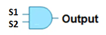
The logic symbol shown is _____.
NOR Gate
OR Gate
NAND Gate
AND Gate
AND gate is represented by switches connected in _____.
series-parallel
parallel
series
all of the choices
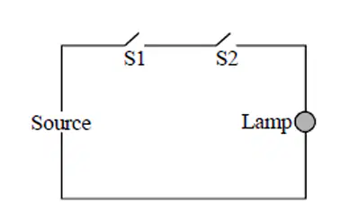
AND gate will only operate when ______
both S1 and S2 are closed
both S1 and S2 are open
S1 is closed
S2 is open
S1 is open
S2 is open
OR gate will only operate when ______
either S1 or S2 or both are closed.
both S1 and S2 are open
What switch/s needs to be closed for the lamp to be OFF?
both S1 and S2 are closed
both S1 and S2 are open
The figure represents _____.
NOT Gate
AND Gate
NAND Gate
NOR Gate
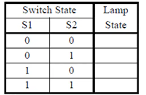
Fill in the truth table below for an AND Gate:
1
1
1
0
0
1
1
1
1
0
0
0
0
0
0
1
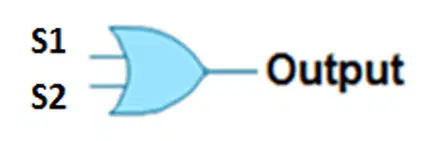
What logic symbol is represented by the figure?
NAND
NOR
AND
OR
OR gate is represented by switches connected in _____.
series
parallel
series-parallel
parallel-series
OR gate will only operate when _____
it is connected to AND gate
both S1 and S2 are open
either S1 or S2 or both are closed
all of the choices
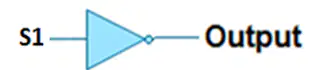
The symbol below is _____.....
AND gate
OR gate
NOT gate
NAND gate
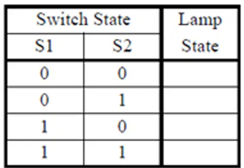
Fill in the truth table for the OR gate:
0
1
1
1
1
0
0
0
1
1
0
0
1
0
0
1
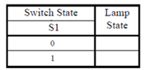
Fill in the truth table for the NOT gate shown:
1
1
0
1
1
0
0
0
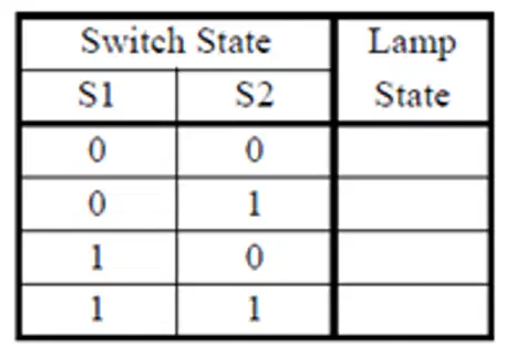
Fill in the truth table for the NAND gate shown:
0
0
0
1
1
1
1
0
1
1
0
0
0
0
1
1
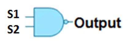
The logic symbol below shows the ____:
AND Gate
NAND Gate
NOR Gate
OR Gate
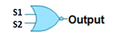
What logic symbol is shown below?
AND
OR
NAND
NOR
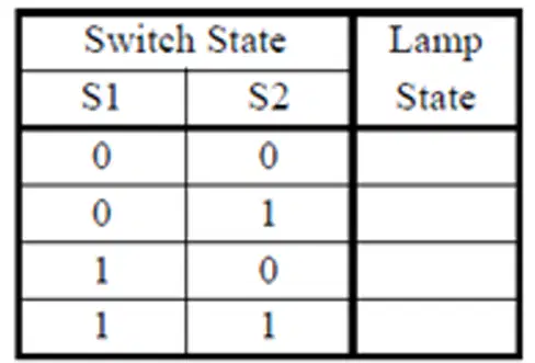
Fill in the truth table below for NOR Gate:
1
0
0
0
0
1
1
1
1
1
1
0
0
0
0
1
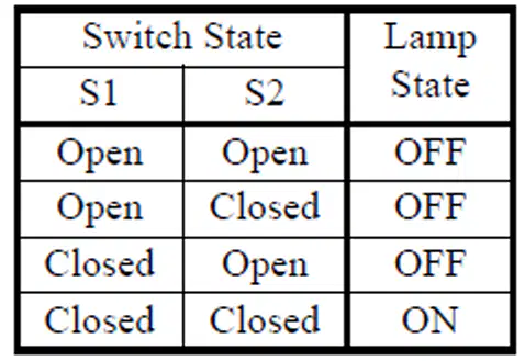
Which logic gate is represented by the TT shown?
NOR
OR
AND
NAND
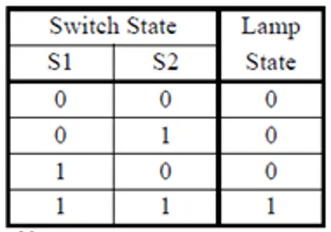
Which logic gate is represented by TT shown?
OR
AND
NOR
EXOR
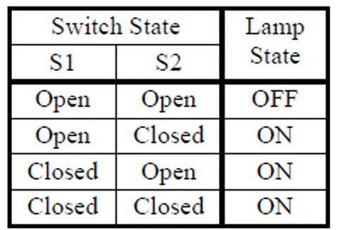
Which logic gate is represented by TT shown?
OR
AND
NOR
EXOR
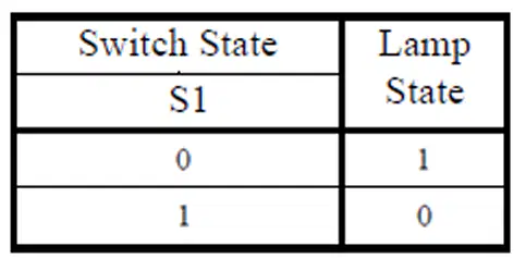
Which logic gate is represented by TT shown?
OR
AND
NOT
EXOR
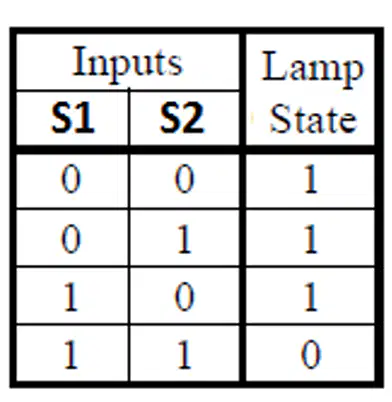
Which logic gate is represented by TT shown?
NOR
NAND
NOT
EXOR
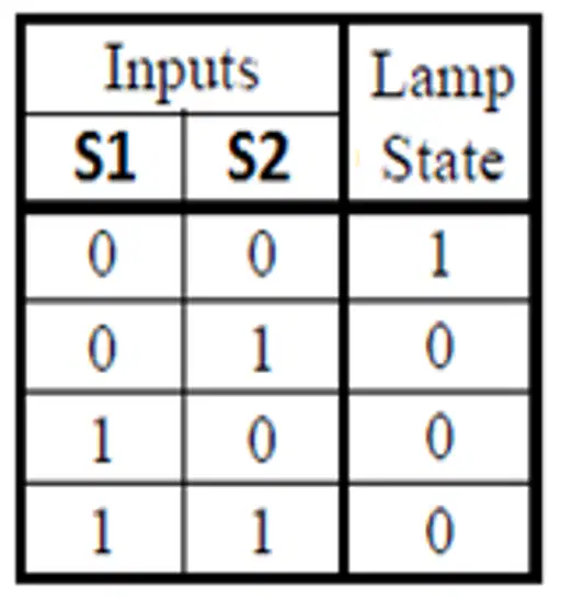
Which logic gate is represented by TT shown?
NOR
NAND
NOT
EXOR
A Schmitt trigger device is one having an output that can be ________
in one of two fixed voltages
both of two fixed voltages
fixed to one voltage
none of the choices
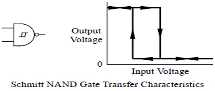
As can be seen from the figure, the output voltage changes ___________ with the change in the input voltage.
incrementally
very slowly
almost instantaneously
all of the choices
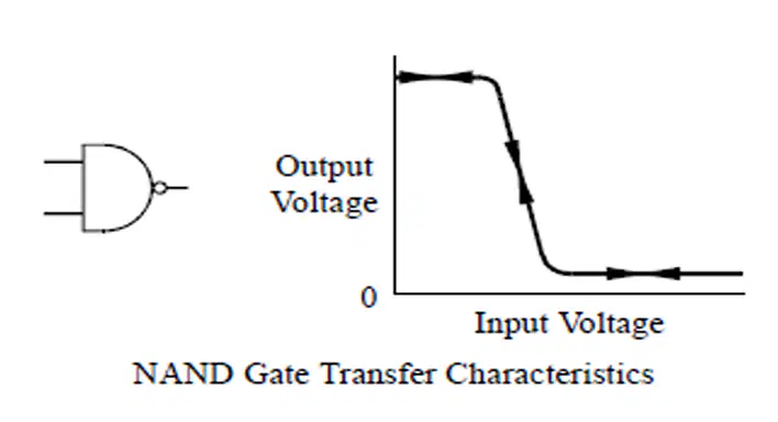
The figure below shows the ____.
NOR Gate Characteristics
AND characteristics
NAND Gate Transfer Characteristics
Schmitt NAND Gate Characteristics
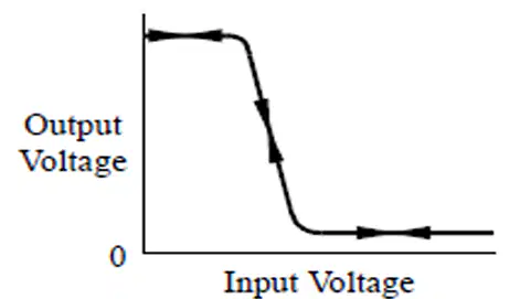
Referring to figure:
___________ with the change in the input voltage.
there is a delay in the output voltage
output voltage changes almost instantaneously
the output voltage is cycling
none of the choices.
The input voltage value at which a change in the output state is triggered is referred to as the _______.
input threshold voltage
peak voltage
open circuit voltage
none of the choices
______ is the difference in voltage between the rising threshold voltage and the falling threshold voltage
voltage difference
potential difference
Hysteresis voltage
none of the choices
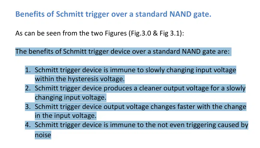
The benefits of Schmitt trigger device over a standard NAND gate are the following: EXCEPT
Schmitt trigger device is not immune to slowly changing input voltage within the hysteresis voltage
Schmitt trigger device does not eliminate noise
Schmitt trigger device output voltage does not changefaster with the change in the input voltage.
Schmitt trigger device is immune to the not even triggering caused by noise
The Boolean expression below is for ______:
Output = S1∘ S2
OR gate
AND gate
NAND gate
XOR Gate
The Boolean expression below is for ______:
Output = S1+ S2
OR gate
AND gate
NAND gate
XOR Gate
The Boolean expression below is for ______:
Output = S1
OR gate
AND gate
NAND gate
NOT gate
The Boolean expression below is for ______:
Output = S1∘S2
OR gate
AND gate
NAND gate
NOT gate
The Boolean expression below is for ______:
Output = S1+S2
OR gate
NOR Gate
NAND gate
NOT gate
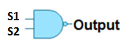
The logic symbol shown is:
AND Gate
NAND Gate
NOR Gate
OR Gate
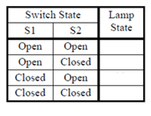
Fill in the truth table below for a EXOR Gate
ON
OFF
ON
OFF
OFF
ON
ON
OFF
OFF
OFF
ON
ON
ON
OFF
OFF
ON
______________are made up from basic logic NAND, NOR or NOT gates that are “combined” or connected together to produce more complicated switching circuits.
Parallel Circuits
Series Circuit
Combinational Circuits
Series Logic Gate Circuits

Identify the logic symbol shown:
EX-NAND
EX-AND
EX-NOR
EX-OR
the EX-OR gate will only operate when _______.
S1 and S2 and S3 are closed
S1 or S2 or both are closed
S1 and S2 are both closed
S1 or S2 are closed but NOT both.
In general, an Ex-OR gate will give an output value of logic “1” ONLY when there are an ________ of 1’s on the inputs to the gate, if the two numbers are equal, the output is “0”.
odd number
even number
equal number
none of the choices
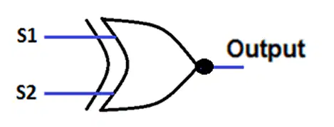
The logic symbol shown is:
EX-NOR
EX-OR
NOR
OR

Fill in the truth table below for EX-NOR gate.
OFF
OFF
ON
ON
ON
OFF
OFF
ON
OFF
ON
ON
OFF
OFF
ON
OFF
ON
______ will only operate when both S1 AND S2 are closed OR both S1 AND S2 are open.
EX-NOR
EX-OR
OR
NOR
As the _______ gives an output of logic level “1” whenever its two inputs are equal.
NOR
NAND
EX-NOR
EX-OR
_______ gates are used in Digital Comparator circuits.
NOR
NAND
EX-NOR
EX-OR
In a decoder, 4 inputs = ____ outputs
16
2
4
8
In a decoder, 4 inputs = ____ outputs
16
2
4
8
What are the number of input lines for an Encoder circuit if it has three (3) number of output lines?
6
3
8
1
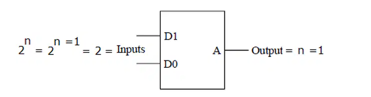
What circuit is indicated by the figure.?
4-2 line decoder
2-1 line decoder
2-1 line encoder
4-2 line encoder
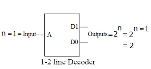
What circuit is indicated by the figure.?
1-2 line decoder
2-1 line decoder
2-1 line encoder
4-2 line encoder

What circuit is indicated by the figure.?
1-2 line decoder
2-4 line decoder
2-1 line encoder
4-2 line encoder
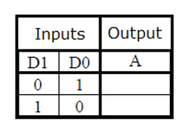
Fill in the truth table for a 2-1 line encoder.
0
0
0
1
1
0
1
0
At any time, _______ can be ‘1’ in order to get the respective binary code at the output line.
both inputs
2 inputs
only one of its input
none of the inputs
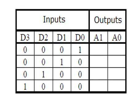
Fill in the truth table below for the 4-2 line decoder.
0 0
0 1
1 0
1 1
0 1
0 0
1 1
1 0
1 1
1 0
0 1
0 0
0 0
1 1
0 1
1 0
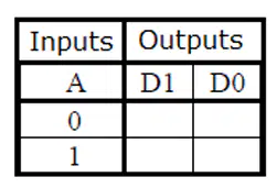
Fill in the truth table below for the 1-2 line decoder.
0 1
1 0
0 0
1 1
1 0
1 0
1 0
0 1

Fill in the truth table below for the 1-2 line decoder.
0 1 0 1
0 1 0 0
0 0 1 1
1 1 1 0
0 0 0 0
1 1 0 0
0 1 0 1
1 1 1 1
0 0 1 0
1 1 0 0
1 0 1 1
0 0 0 1
0 0 0 1
0 0 1 0
0 1 0 0
1 0 0 0
A Half adder circuit is a __________that can add two “one-bit binary” numbers from its two inputs
logic comparison circuit
binary adding circuit
binary subtractor circuit
multiplexer circuit
A Half Adder circuit is made from an EX-OR gate providing the SUM output of the inputs “A & B” and an _______________.
NOT gate providing the SUM output
NAND gate providing the CARRY output
AND gate providing the CARRY output
OR gate providing the CARRY output
A single-bit full adder circuit can be made by two HALF ADDER circuits and an _______
NAND gate
OR gate
NOR gate
AND gate
A full adder circuit is a binary adding circuit that performs an addition operation on ________ numbers
three one-bit binary
two one-bit binary
one one-bit binary
four one-bit binary
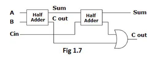
What does the diagram here show?
half-subtractor
full-subtractor
half-adder
full-adder
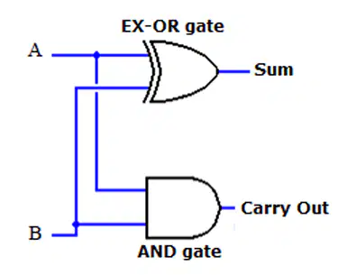
What circuit is shown:
Full-adder circuit
half-adder circuit
half-subtractor circuit
full-subtractor circuit
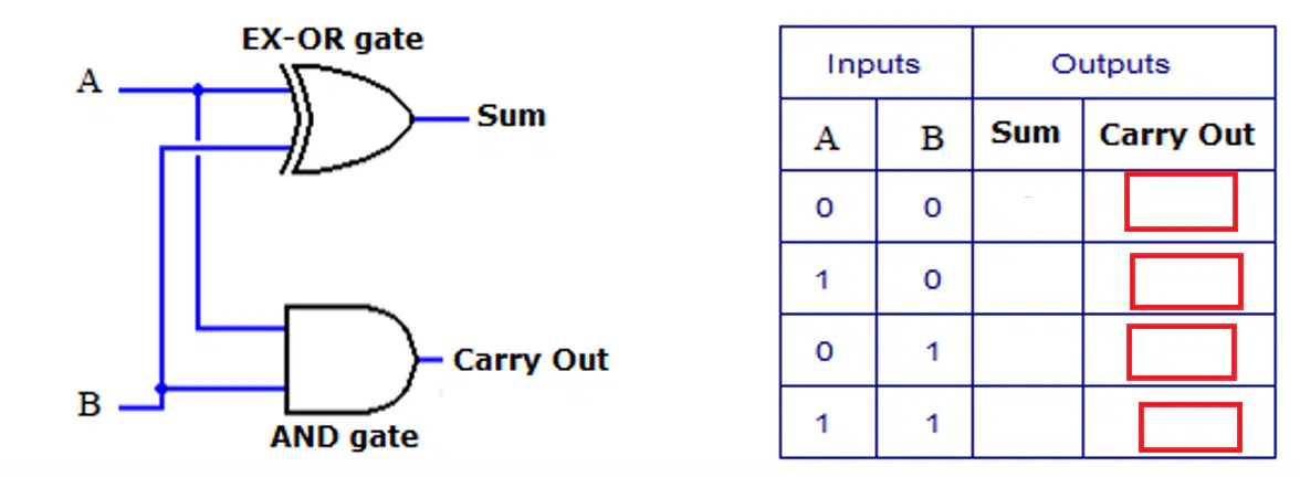
fill in the truth table below for the half-adder circuit
1 1
0 1
0 0
1 0
1 0
1 0
0 0
0 1
0 0
1 0
1 0
0 1
0 0
1 1
0 1
1 0
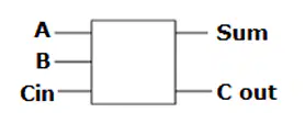
WHat figure is shown?
full adder
half adder
full subtractor
half subtractor
a ______ can add three “one-bit binary” numbers from its three inputs “A, B & Cin”
full-subtractor
half adder
full-adder
half-subtractor
What is one advantage of full-adder circuit?
It is capable of producing an output of SUM and CARRY-OUT
It eliminates the need for logic gates
It can only add one-bit binary numbers
It requires no input carry
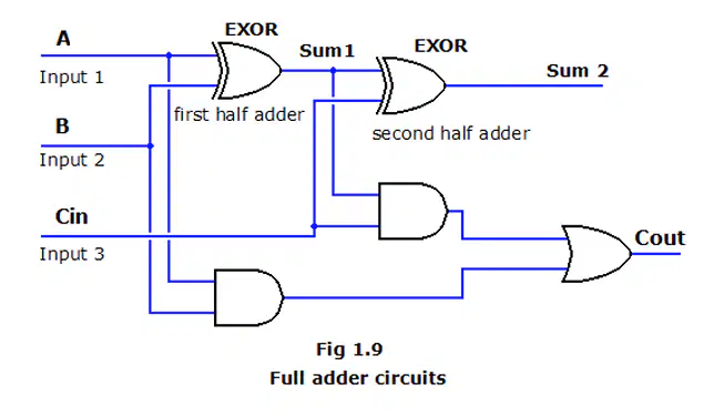
Refer to figure.
the Cout will only be at logical 1, _________
if only one of the inputs is high
if any of the two inputs (A, B & Cin) OR all of the three are HIGH.
if all inputs are low
if one input is high and 2 inputs are low
In JK flipflop, J stands for _____ and K stands for _____.
set, set
clear, set
set, clear
clear, clear
In JK Flipflop, what does CLK stand for?
clock input terminal (clock pulse)
clicking pulse
output terminal
clock battery
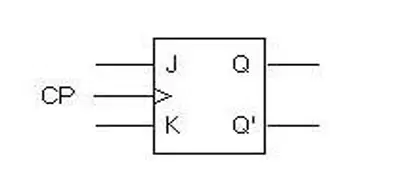
what is the figure shown below?
D FLip FLop
SR Flip Flop
JK Flip FLop
none of the choices
J-K flip-flop circuit can be made using _________
2 NAND gates
3 NAND gates
4 NAND gates
3 NOR gates
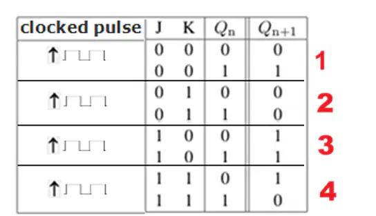
This is the truth-table for JK Flip Flop.
Determine the outputs 1/2/3/4
1 - No change
2 - reset
3 - Set
4 - Toggle
1 - reset
2 -toggle
3 - no change
4 - set
1 - toggle
2 - reset
3 - no change
4 - Toggle
1 - reset
2 - set
3 - no change
4 - Toggle
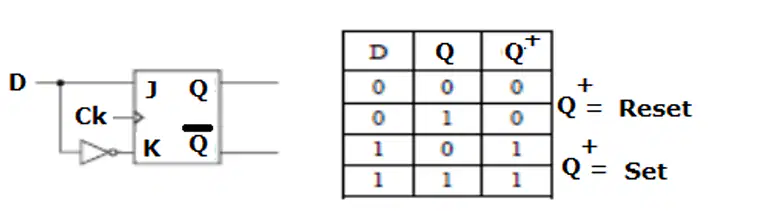
this figure shows a JK flip flop converted to a ________.
none of the choices
D type and its truth table
SR type and its truth table
A type and its lies table
The D Type flip flop is a slight modification of the J-K flip flop by inserting an ______ between J and K
inverter
AND gate
NAND gate
NOR gate
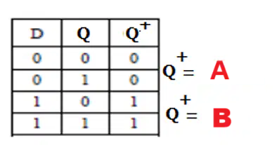
what do the following outputs stand for?
1 - reset
2 - set
1 - set
2 - reset
1 - set
2 - set
1 - reset
2 - reset
When groups of these devices are connected together and used to store digital data they are referred to as _____
phrases
sentences
registers
paragraphs
The complete data stored by the group is referred to as a _______
word
letter
register
alphabet
A register enabling shifting of the bits within the register is referred to as a _______.
JK flipflop
shift register
register card
word
Shift registers can be constructed using clocked D-type or ______.
1 OR gate
2 NAND gates
JK Flip Flops
D flip flops
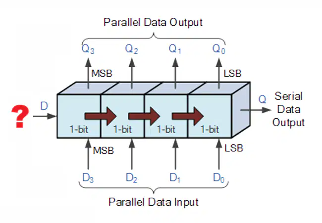
What is "A"?
SIPO
PISO
SISO
PIPO
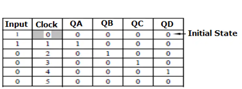
after the 5th clock pulse is generated, ______.
the input to D-type A is at logic 1
it will have been shifted completely out of the register.
the input to D-type A is at logic 1 and this will be transferred to its output QA.
the input to D-type A is at logic 0
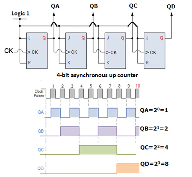
the count output after the 6th clock pulse is ______
0000
1000
0110
1010
the count output after the 7th clock pulse is ______
0000
1000
0111
1010
the count output after the 8th clock pulse is ______
0000
1000
1110
1010
The total output from the shift register shown is:
15
8
4
2
110111 to decimal = ____....
157
63
115
119
sequential circuit that loads the data present on its inputs and then moves or “shifts” it to its output once every clock cycle
closed circuit
shift register
encoder
decoder
_____________ Shift Register circuit, is a circuit that moves/shift the data serially “IN” and “OUT” one bit at a time under clock control
SIPO
SISO
PISO
PIPO
Hex A3 to decimal?
153
161
163
173
255 decimal to HEX
FF
FE
EF
F1
Decimal 93 to BCD
1001 0011
1001 1001
1001 0101
1001 1000
decimal 150 --> binary
10010110
10010100
10011010
10011110
10111100 to decimal
188
184
192
186
octal 75 to decimal
61
65
77
53
72 to binary
1001000
111000
100110
110010

