
 Worksheets
Electronic Devices Test-2 (JFET,SCR,LED,SSD,LDR&PhotoDiode)
Total questions: 80
Worksheet time: 45mins
Name
Class
Date
1.
Name of the Student
4 lines
2.
Roll Number of the Student
4 lines
3.
The BJT is a ________ device. The FET is a ________ device.
a)
bipolar, bipolar
b)
bipolar, unipolar
c)
unipolar, bipolar
d)
unipolar, unipolar
4.
A field effect transistor operates on
a)
Majority carriers only
b)
Minority carriers only
c)
Positively charged ions only
d)
Negatively charged ions only
5.
What is the level of drain current ID for gate-to-source voltages VGS less than (more negative than) the pinch-off level?
a)
zero amperes
b)
IDSS
c)
Negative value
d)
Undefined
6.
What is the ratio of ID / IDSS for VGS = 0.5 VP?
a)
0.25
b)
0.5
c)
1
d)
0
7.
Which of the following represent(s) the cutoff region for an FET?
a)
ID = 0 A
b)
ID = IDSS
c)
ID = IDSS/2
d)
ID = IDSS/4
8.
Which of the following controls the level of ID?
a)
VGS
b)
VDS
c)
IG
d)
VDG
9.
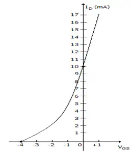
Referring to the following transfer curve, determine the level of VGS when the drain current is 10 mA.
a)
0 V
b)
–1.66 V
c)
0.66 V
d)
–0.66 V
10.
With a JFET, a ratio of output current change against an input voltage change is called
a)
Transconductance
b)
Impedance
c)
Resistivity
d)
Gain
11.
In the constant-current region, how will the ID change in an n-channel JFET?
a)
As VGS varies ID varies.
b)
As VGS decreases ID remains constant
c)
As VGS increases ID remains constant
d)
As VDS varies ID varies.
12.
A JFET is a ………… driven device
a)
Current
b)
Voltage
c)
Current or voltage
13.
In a JFET, when drain voltage is equal to pinch-off voltage, the depletion layers ………
a)
almost touch each other
b)
have large gap
c)
have moderate gap
14.
For constant VDS, if VGS is changed from 0V to -1V, the drain current
a)
Decreases
b)
Increases
c)
Remains constant
d)
Becomes zero
15.
The pinch off voltage is the
a)
Gate to source voltage when drain current is maximum
b)
Drain to source voltage when drain current is zero
c)
Drain to source voltage when drain current is maximum
d)
Gate to source voltage when drain current is half of maximum current
16.
A certain JFET data sheet gives VGS(off) = -4 V. The pinch-off voltage Vp is ……..
a)
+4 V
b)
-4 V
c)
dependent on VGS
d)
data insufficient
17.
A JFET has a driven current of 4 mA. If IDSS = 8 mA and VGS(off)= -6 V. Find the values of VGS and VP.
a)
-1.76 V, 6 V
b)
6 V, 1.86 V
c)
-1.76 V, -6 V
d)
1.86 V, 6 V
18.
An N-channel JFET has IDSS = 8 mA and VGS(off)= -5 V. Determine the drain current ID for VGS = -2 V.
a)
2.5 mA
b)
2 mA
c)
2.3 mA
d)
2.88 mA
19.
An N-channel JFET has IDSS = 10 mA and VGS(off)= -4 V. determine the minimum value of VDS for pinch-off and drain current ID for VGS= -2 V in pinch-off region.
a)
2.5 V, 2.5 mA
b)
4 V, 2.5 mA
c)
3 V, 3 mA
d)
2.5 V, 3 mA
20.
Determine the magnitude of gm for a JFET with IDSS= 8 mA and VGS(off)= -4 V when VGS is changed from VGS= -1.5V to VGS= -2.5 V.
a)
2 m mho
b)
4 m mho
c)
1.5 m mho
d)
2.5 m mho
21.

Calculate the transconductance (gm) between the points A and B from the graph shown
a)
2 mS
b)
0.3 mS
c)
3 mS
d)
5 mS
22.
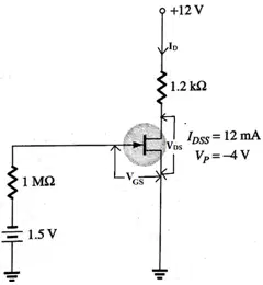
For the fixed bias configuration of figure given below, determine VGS, ID and VDS.
a)
-1.5 V, 4.69 mA, 6.372 V
b)
-1.0 V, 6.21 mA, 7.372 V
c)
-1.2 V, 5.08 mA, 6.372 V
d)
-2 V, 4.69 mA, 7.523 V
23.
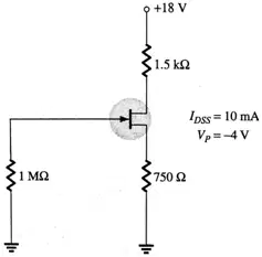
For the circuit shown in figure, find ID, VGS and VDS
a)
10 mA, -4 V, 12.13 V
b)
2.61 mA, -1.96 V, 12.13 V
c)
2.61 mA, 18 V, -4 V
d)
3.65 mA, 1.96 V, 18 V
24.
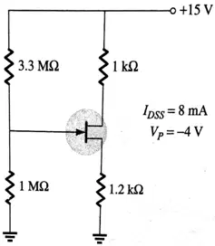
For the circuit shown find ID, VGS, VDS and gm
a)
8 mA, -4 V, 7.5 V, 2 m mho
b)
3.91 mA, -1.2 V, 6.398 V, 2.8 m mho
c)
3.5 mA, -2 V, 8 V, 0.5 m mho
d)
4 mA, -1 V, 15 V, 3.8 m mho
25.
An SCR has …………….. pn junctions.
a)
Two
b)
Three
c)
Four
d)
None of the above
26.
An SCR has ………….. semiconductor layers.
a)
Two
b)
Three
c)
Four
d)
None
27.
An SCR has three terminals viz …………….
a)
Cathode, anode, gate
b)
Anode, cathode, grid
c)
Anode, cathode, drain
d)
None of the above
28.
An SCR behaves as a ……………. switch.
a)
Unidirectional
b)
Bidirectional
c)
Mechanical
d)
None of the above
29.
An SCR is a…………
a)
Triac
b)
Diac
c)
Unijunction transistor
d)
Thyristor
30.
An SCR is made of ………….
a)
Germanium
b)
Silicon
c)
Carbon
d)
None of the above
31.
In the normal operation of an SCR, anode is …………… w.r.t. cathode.
a)
At zero potential
b)
Negative
c)
Positive
d)
None of the above
32.
An SCR combines the features of …………..
a)
A rectifier and resistance
b)
A rectifier and transistor
c)
A rectifier and capacitor
33.
The control element of an SCR is ………….
a)
Gate
b)
Anode supply
c)
Anode
d)
Cathode
34.
One of the ways to turn on a SCR is by supplying……………..
a)
Breakover voltage
b)
Appropriate anode current
c)
Knee voltage
d)
None of the above
35.
An SCR is turned off by …………….
a)
Reducing anode voltage to zero
b)
Reducing gate voltage to zero
c)
Reverse biasing the gate
d)
None of the above
36.
An SCR is a ……………….. triggered device.
a)
Voltage
b)
Current
c)
Voltage as well as current
37.
When an SCR is turned on, the voltage across it is about ……….
a)
Zero
b)
10 V
c)
1 V
d)
20 V
38.
An SCR is turned off when …………..
a)
Anode current is reduced below holding current
b)
Gate voltage is reduced to zero
c)
Gate is reverse biased
d)
None of the above
39.
In an SCR circuit, the angle of conduction can be changed by ………
a)
Changing anode voltage
b)
Changing gate voltage
c)
Reverse biasing the gate
d)
None of the above
40.
If gate current is increased, then anode-cathode voltage at which SCR conducts …………….
a)
Is decreased
b)
Is increased
c)
Remains the same
d)
None of the above
41.
When SCR is reverse biased, the current is …………….
a)
Exactly zero
b)
Small leakage current
c)
Large leakage current
d)
None of the above
42.
When SCR starts conducting, then ……………. loses all control
a)
Gate
b)
Cathode
c)
Anode
d)
None of the above
43.
Light emitting diode(LED) is a
a)
A) Display device
b)
B) Storing device
c)
C) Zener diode
d)
D) Voltage regulator
44.
Radiation emitted by Light emitting diode(LED) can be seen in the
a)
A) Visible spectrum
b)
B) infrared region
c)
C) ultraviolet region
d)
D) Visible as well as infrared region
45.
LEDs that radiate infrared rays are manufactured by using
a)
A) arsenide phosphide
b)
B) gallium phosphide
c)
C) gallium arsenide phosphide
d)
D) gallium arsenide
46.
Efficiency of an LED for generating light is directly proportional to
a)
A) temperature
b)
B) voltage applied
c)
C) level of doping used
d)
D) current injected
47.
The injection process in the LED is
a)
A) minority carrier injection
b)
B) majority carrier injection
48.
The colour of LED depends on
a)
A) heat evolved
b)
B) energy involved
c)
C) colour used
49.
LEDs are devices with the power in the range of
a)
A) kilowatt
b)
B) watt
c)
C) megawatt
d)
D) milliwatt
50.
A good material for LED should have energy gap in the
a)
A) UV range
b)
B) Visible range
c)
C) IR range
51.
The light emitted by the LED is a function of the
a)
A) voltage
b)
B) temperature
c)
C) current
52.
LEDs are ____ biased for their normal operation
a)
A) forward
b)
B) reverse
c)
C) either forward or reverse
53.
The output colour of the GaAs LED is
a)
A) yellow
b)
B) green
c)
C) amber
d)
D) red
54.
LED’s efficiency is a measure of electrical energy required to produce a certain
a)
A) current
b)
B) resistance
c)
C) light output
55.
For the GaAsP red the wavelength lies in the range between
a)
A) 600 and 700 nm
b)
B) 550 and 650 nm
c)
C) 700 and 750 nm
d)
D) None
56.

Refer to below figure, Which symbol is correct for an LED?
a)
A. a
b)
B. b
c)
C. c
d)
D. d
e)
E. e
57.
An LED is forward-biased. The diode should be on, but no light is showing. A possible trouble might be
a)
A. forward voltage is below the knee voltage of diode.
b)
B. the series resistor is too small.
c)
C. none. The diode should be off if forward-biased.
d)
D. the power supply voltage is too high
58.
Features of LED are a) Invisible in darkness b) Needs very less power c) Operating voltage range is 1.5 V to 5V dc. d) Operating in forward biased condition only. Correct statements are:
a)
(A) a,d
b)
(B) b,c,d
c)
(C) All the above
59.
Seven-segment display uses seven individual
a)
A. light emitting diodes
b)
B. light restoring diodes
c)
C. capacitors
d)
D. inductors
60.
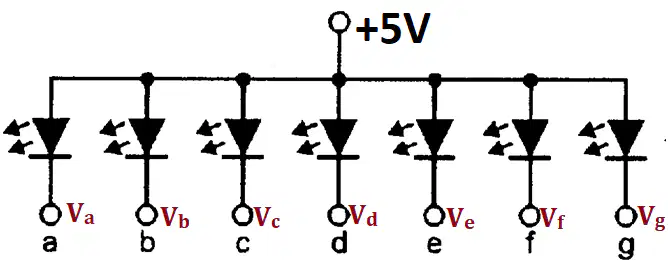
Which digit will be displayed when Va = Vb= Vd = Ve= Vg = 0 V and other terminals are at 5V ?
a)
A. 0
b)
B. 7
c)
C. 2
d)
D. 5
61.
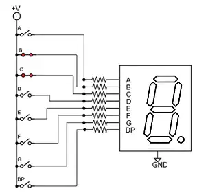
The digit displaying in the below CA arrangement is
a)
A. 0
b)
B. 7
c)
C. 1
d)
D. 5
62.
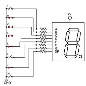
The digit displaying in the below CC arrangement is
a)
A. 0
b)
B. 6
c)
C. 2
d)
D. d
63.
Photoconductive devices are made of
a)
A) Highly conductive material
b)
B) Semiconductor material
c)
C) Radioactive material
d)
D) Photo resistive device
64.
Light dependent resistor is a type of
a)
A) Photovoltaic device
b)
B) Photo-emissive device
c)
C) Radioactive device
d)
D) Photo resistive device
65.
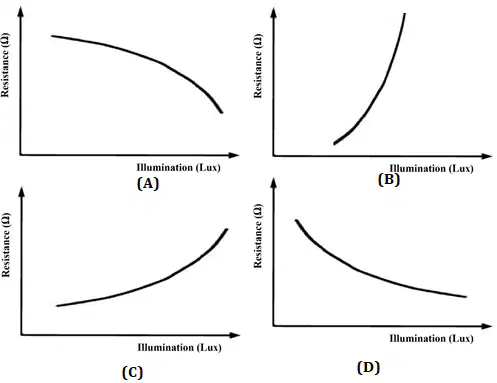
Variation of resistance with light intensity for LDR is represented by
a)
A
b)
B&C
c)
D
d)
all the above
66.
Solar cell is a type of
a)
A) Photovoltaic device
b)
B) Photoemissive device
c)
C) Electromotive device
67.
Light dependent resistor behaves like a
a)
A) Capacitor
b)
B) Dielectric medium
c)
C) Switch
d)
D) Battery
68.
Photodiode is a type of
a)
A) Light dependent resistor
b)
B) Photoemissive device UI
c)
C) Semiconductor pn junction diode
69.
In case a reverse biased photodiode is kept in dark condition, the current flowing through the device corresponds to
a)
A) Maximum value of current flowing through the device
b)
B) Reverse saturation current
c)
C) Normal value of current
d)
D) Zero
70.
Phototransistor connected in a circuit generally in
a)
A) CB configuration
b)
B) CE configuration
c)
C) CC configuration
d)
D) Any of the above
71.
Sensitivity of a phototransistor as compared to any other photosensitive semiconductor device is
a)
A) The same
b)
B) Slightly less
c)
C) Slightly more
d)
D) Much more
72.
A photovoltaic cell is
a)
A) A photodiode without reverse bias voltage
b)
B) Type of phototransistor
c)
C) Light dependent resistor
d)
D) A photodiode with reverse bias voltage
73.
The value of dark-current of a photoconductive cell is
a)
A) negligibly small
b)
B) very high
c)
C) zero
d)
D) high
74.
If the reverse voltage across the photodiode is increased, the width of depletion region
a)
A) decreases
b)
B) remains the same
c)
C) increases
75.
Variation of current w.r.t the illumination flux in the photo diode is
a)
A) linear
b)
B) exponential
c)
C) circular
d)
D) parabolic
76.
If the luminous flux is increased, the internal resistance of photovoltaic cell
a)
A) decreases
b)
B) remains the same
c)
C) increases
77.
Photoconductive compound used in LDR is
a)
A) CdS
b)
B) Ni
c)
C) cobalt oxide
d)
D) GaAsP
78.
Dark resistance of the LDR is of the order of
a)
A) kiloohm
b)
B) ohm
c)
C) megaohm
d)
D) milliohm
79.
Drawback of LDR is that its resistance is dependent on
a)
A) current
b)
B) temperature
c)
C) material used
d)
D) none
80.
The process of emitting photons from a semi conductor material is called
a)
A. photoluminescence.
b)
B. gallium arsenide.
c)
C. electroluminescence.
d)
D. gallium phosphide
100 %

