
 Worksheets
ELECS 2
Total questions: 200
Worksheet time: 2hrs 40mins
Name
Class
Date
1.
A silicon diode measures a low value of resistance with the meter leads in both positions. The trouble, if any, is
a)
the diode is open
b)
the diode is working correctly.
c)
the diode is internally shorted
d)
the diode is shorted to ground.
2.
Under normal conditions a diode conducts current when it is
a)
avalanched.
b)
forward-biased.
c)
saturated.
d)
reverse-biased.
3.
As the forward current through a silicon diode increases, the internal resistance
a)
decreases.
b)
increases.
c)
remains the same.
d)
NOTA
4.
For a forward-biased diode, the barrier potential ________ as temperature increases.
a)
increases.
b)
remains the same.
c)
NOTA
d)
decreases.
5.
An n-type semiconductor material
a)
has pentavalent impurity atoms added.
b)
is intrinsic.
c)
requires no doping.
d)
has trivalent impurity atoms added.
6.
Which statement best describes an insulator?
a)
A material with few free electrons.
b)
A material doped to have some free electrons.
c)
No description fits
d)
A material with many free electrons.
7.
The boundary between p-type material and n-type material is called
a)
a pn junction
b)
a diode.
c)
a reverse-biased diode.
d)
a forward-biased diode.
8.
An ideal diode presents a(n) ________ when reversed-biased and a(n) ________ when forward-biased.
a)
open, short
b)
short, short
c)
open, open
d)
short, open
9.
What types of impurity atoms are added to increase the number of conduction-band electrons in intrinsic silicon?
a)
trivalent
b)
octavalent
c)
pentavalent
d)
bivalent
10.
An atom is made up of
a)
all of the above
b)
electrons.
c)
protons
d)
neutrons.
11.
There is a small amount of current across the barrier of a reverse-biased diode. This current is called
a)
conventional current.
b)
reverse breakdown current.
c)
forward-bias current.
d)
reverse leakage current.
12.
Doping of a semiconductor material means
a)
that impurities are added to increase the resistance of the material.
b)
that impurities are added to decrease the resistance of the material.
c)
that all impurities are removed to get pure silicon.
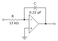
d)
that a glue-type substance is added to hold the material together.
13.
The most common type of diode failure is a(n) ________.
a)
short
b)
NOTA
c)
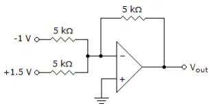
resistive
d)
open
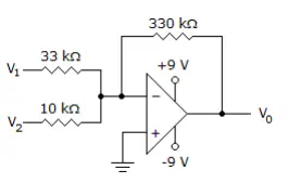
14.
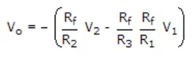
Zener diodes with breakdown voltages less than 5 V operate predominantly in what type of breakdown?
a)
Schottky
b)
Varactor
c)
Avalanche
d)
Zener
15.
You have an application for a diode to be used in a tuning circuit. A type of diode to use might be
a)
a Schottky diode.
b)
a LED.
c)
a Gunn diode.
d)
a varactor
16.
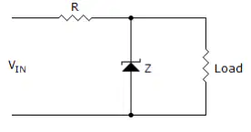
Refer to this figure. If VIN increases, IZ will
a)
remains the same.
b)
decrease
c)
NOTA
d)
increase
17.
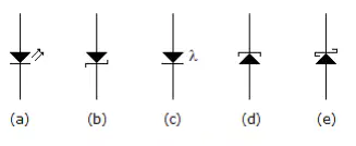
Refer to this figure. Which symbol is correct for a zener diode?
a)
B
b)
C
c)
D
d)
A
18.
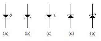
Refer to the figure at 17. Identify the Schottky diode.
a)
E
b)
A
c)
D
d)
B
19.
The normal operating region for a zener diode is the
a)
reverse-bias region.
b)
zero-crossing region.
c)
forward-bias region.
d)
reverse-breakdown region
20.
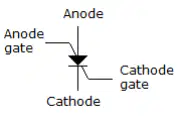
An LED is forward-biased. The diode should be on, but no light is showing. A possible trouble might be
a)
the series resistor is too small.
b)
the power supply voltage is too high.
c)
none. The diode should be off if forward-biased.
d)
the diode is open.
21.
What diode operates only with majority carriers?
a)
step-recovery
b)
Schottky
c)
Tunnel
d)
Laser
22.
What type of diode maintains a constant current?
a)
Pin
b)
Zener
c)
Current regulator
d)
LED
23.
Refer to the figure in number 16. If VIN decreases, IR will
a)
decrease
b)
remains the same.
c)
increase
d)
NOTA
24.
Back-to-back varactor diodes are used for what reason?
a)
no reason; only zeners are used in a back-to-back configuration
b)
over-voltage protection
c)
a wider tuning range
d)
to eliminate harmonic distortion
25.
What type of diode is commonly used in electronic tuners in TVs?
a)
LED
b)
Schottky
c)
Gunn
d)
Varactor
26.
A varactor is a pn junction diode that always operates in ________-bias and is doped to ________ the inherent capacitance of the depletion region.
a)
forward, maximize
b)
reverse, minimize
c)
reverse, maximize
d)
forward, minimize
27.

Refer to this figure. Determine the minimum value of IB that will produce saturation.
a)
10.425 uA
b)
0.25 mA
c)
1.065 uA
d)
5.325 uA
28.
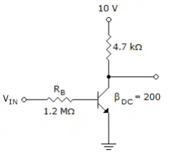
Refer to the figure at 27. If VCE = 0.2 V, IC(sat) is:
a)
1.065 mA
b)
7.4 mA
c)
2.085 mA
d)
0.05 mA
29.
For normal operation of a pnp BJT, the base must be ________ with respect to the emitter and ________ with respect to the collector.
a)
negative, negative
b)
negative, positive
c)
positive, positive
d)
positive, negative
30.
When a transistor is used as a switch, it is stable in which two distinct regions?
a)
active and cutoff
b)
saturation and active
c)
saturation and cutoff
d)
none of the above
31.
For a silicon transistor, when a base-emitter junction is forward-biased, it has a nominal voltage drop of
a)
VCC
b)
0.3 V
c)
0.7 V
d)
0.2 V
32.
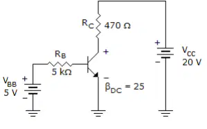
Refer to this figure. The value of VCE is:
a)
9.9 V
b)
0.7 V
c)
9.2 V
d)
19.3 V
33.
A BJT has an IB of 50uA and a BDC of 75; IC is:
a)
3.75 mA
b)
37.5 mA
c)
375 mA
d)
0.375 mA
34.
What are the two types of bipolar junction transistors?
a)
ppn and nnp
b)
pnn and nnp
c)
pts and stp
d)
npn and pnp
35.
The value of BDC
a)
is fixed for any particular transistor.
b)
varies with temperature and IC.
c)
varies with IC.
d)
varies with temperature.
36.
What is the ratio of IC to IE?
a)
either BDC/(BDC+1) or aDC, but not BDC
b)
BDC
c)
aDC
d)
BDC/(BDC+1)
37.
In what range of voltages is the transistor in the linear region of its operation?
a)
none of the above
b)
0 < VCE
c)
0.7 < VCE
d)
VCE(max) > VCE
38.
What is (are) general-purpose/small-signal transistors case type(s)?
a)
TO-39
b)
all of the above
c)
TO-92
d)
TO-18
39.
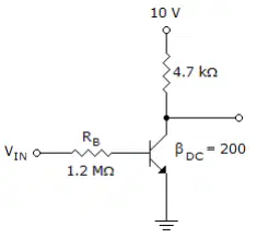
Refer to the figure in 27. Determine the minimum value of VIN from the following that will saturate this transistor.
a)
13.21 V
b)
0.7 V
c)
12.51 V
d)
9.4 V
40.
How many layers of material does a transistor have?
a)
1
b)
3
c)
2
d)
4
41.
In the active region, while the collector-base junction is ________-biased, the base-emitter is ________-biased.
a)
reverse, forward
b)
forward, reverse
c)
forward, forward
d)
reverse, reverse
42.
What range of resistor values would you get when checking a transistor for forward- and reverse-biased conditions by an ohmmeter?
a)
Exceeding 100kΩ, exceeding 100 kΩ
b)
100 to a few kΩ, 100 to a few kΩ
c)
100Ω to a few kΩ, exceeding 100 kΩ
d)
Exceeding 100kΩ, 100 to a few kΩ
43.
In which region are both the collector-base and base-emitter junctions forward-biased?
a)
All of the above
b)
Cutoff
c)
Active
d)
Saturation
44.
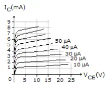
Use this table of collector characteristics to calculate Bac at VCE = 15 V and IB = 30 uA.
a)
50
b)
106
c)
400
d)
100
45.
What does a reading of a large or small resistance in forward- and reverse-biased conditions indicate when checking a transistor using an ohmmeter?
a)
Faulty device
b)
Good device
c)
None of the above
d)
Bad ohmmeter
46.
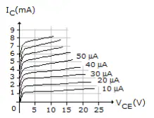
In figure 44, calculate Bdc at VCE = 15 V and IB = 30 uA.
a)
110
b)
50
c)
100
d)
116
47.
Which of the following can be obtained from the last scale factor of a curve tracer?
a)
hFE
b)
αdc
c)
αac
d)
Bac
48.
What are the ranges of the ac input and output resistance for a common-base configuration?
a)
50 kΩ –1 MΩ, 10Ω –100Ω
b)
10 –100 Ωk, 50Ω –1 kΩ
c)
10 –100Ω , 50 kΩ –1 MΩ
d)
None of the above
49.
What is the most frequently encountered transistor configuration?
a)
Emitter-collector
b)
Common-collector
c)
Common-emitter
d)
Common-base
50.
How many individual pnp silicon transistors can be housed in a 14-pin plastic dual-in-line package?
a)
10
b)
7
c)
4
d)
14
51.
In what decade was the first transistor created?
a)
1950s
b)
1960s
c)
1930s
d)
1940s
52.
What is the ratio of the total width to that of the center layer for a transistor?
a)
15:1
b)
1:15
c)
1:150
d)
150:1
53.
Which of the h-parameters corresponds to re in a common-base configuration?
a)
hfb
b)
hib
c)
hrb
d)
hob
54.
Which of the following conditions must be met to allow the use of the approximate approach in a voltage-divider bias configuration?
a)
Bre< 10R2
b)
BRE < 10R2
c)
BRE > 10R2
d)
Bre> 10R2
55.
What is the typical value of the current gain of a common-base configuration?
a)
Undefined
b)
Between 1 and 50
c)
Between 100 and 200
d)
Less than 1
56.
The ________ model fails to account for the output impedance level of the device and the feedback effect from output to input.
a)
hybrid equivalent
b)
re
c)
Thevenin
d)
Beta
57.
What is the voltage gain of a feedback pair connection?
a)
100
b)
-100
c)
1
d)
-1
58.
The advantage that a Sziklai pair has over a Darlington pair is
a)
higher input impedance.
b)
higher current gain.
c)
higher voltage gain.
d)
less input voltage is needed to turn it on.
59.
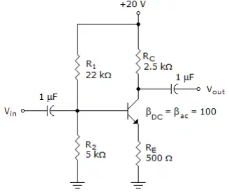
Refer to this figure. Calculate the value of Rin(tot).
a)
2.25 kΩ
b)
378 Ω
c)
37.7 kΩ
d)
3.77 kΩ
60.
For the common-emitter fixed-bias configuration, there is a ________ phase shift between the input and output signals.
a)
0º
b)
90º
c)
45º
d)
180º
61.
The differential amplifier has
a)
two inputs and two outputs.
b)
one input and two outputs.
c)
one input and one output.
d)
two inputs and one output.
62.
The ________ model suffers from being limited to a particular set of operating conditions if it is to be considered accurate.
a)
hybrid equivalent
b)
re
c)
Beta
d)
Thevenin
63.
The ________ configuration is frequently used for impedance matching.
a)
emitter-follower
b)
voltage-divider bias
c)
fixed-bias
d)
collector feedback
64.
In a common-base amplifier, the input signal is connected to the
a)
output.
b)
collector.
c)
base.
d)
emitter.
65.
For the common-emitter amplifier ac equivalent circuit, all capacitors are
a)
connected to ground.
b)
effectively open circuits.
c)
not connected to ground.
d)
effectively shorts.
66.
Which of the following gains is less than 1 for a common-base configuration?
a)
Ai
b)
None of the above
c)
Ap
d)
Av
67.
Which of the following should be done to obtain the ac equivalent of a network?
a)
All of the above
b)
Replace all capacitors by a short-circuit equivalent.
c)
Set all dc sources to zero
d)
Remove all elements bypassed by the short-circuit equivalent.
68.
For the collector dc feedback configuration, there is a ________ phase shift between the input and output signals.
a)
90º
b)
180º
c)
0º
d)
45º
69.
Which of the following configurations has an output impedance Zo equal to RC?
a)
Common-emitter voltage-divider without bypass capacitor
b)
All of the above
c)
Common-emitter voltage-divider with bypass capacitor
d)
Fixed-bias common-emitter
70.
For BJT amplifiers, the ________ gain typically ranges from a level just less than 1 to a level that may exceed 1000.
a)
All of the above
b)
current
c)
impedance
d)
voltage
71.
An emitter-follower amplifier has an input impedance of 107 kΩ. The input signal is 12 mV. The approximate output voltage is (common-collector)
a)
8.92 V
b)
8.9 mV
c)
112 mV
d)
12 mV
72.
What is the limit of the efficiency defined by = Po / Pi?
a)
Greater than 1
b)
Always 1
c)
None of the above
d)
Less than 1
73.
Which of the following techniques can be used in the sinusoidal ac analysis of transistor networks?
a)
Small- or large-signal
b)
Large-signal
c)
Small-signal
d)
None of the above
74.
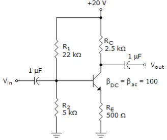
Refer to the figure in 59. If an emitter bypass capacitor was installed, what would the new Av be?
a)
4.96
b)
125
c)
600
d)
398
75.
A Darlington pair amplifier has
a)
low input impedance and low voltage gain.
b)
a voltage gain of about 1 and a low input impedance.
c)
high input impedance and high voltage gain.
d)
a low voltage gain and a high input impedance.
76.
What is the level of drain current ID for gate-to-source voltages VGS less than (more negative than) the pinch-off level?
a)
IDSS
b)
Undefined
c)
zero amperes
d)
Negative value
77.
What is the range of an FET's input impedance in Ω?
a)
10 to 1 k
b)
1 k to 10 k
c)
50 k to 100 k
d)
1 M to several hundred M
78.
At which of the following condition(s) is the depletion region uniform?
a)
No bias
b)
None of the above
c)
VDS > 0 V
d)
VDS = VP
79.
Which of the following controls the level of ID?
a)
IG
b)
VGS
c)
VDS
d)
VDG
80.
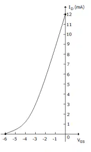
Referring to this transfer curve. Calculate (using Shockley's equation) VGS at ID = 4mA.
a)
–12 V
b)
–2.54 V
c)
Undefined
d)
2.54 V
81.
The transfer curve is not defined by Shockley's equation for the ________.
a)
JFET
b)
BJT
c)
depletion-type MOSFET
d)
enhancement-type MOSFET
82.
The region to the left of the pinch-off locus is referred to as the ________ region.
a)
saturation
b)
cutoff
c)
ohmic
d)
All of the above
83.
Which of the following transistor(s) has (have) depletion and enhancement types?
a)
MOSFET
b)
BJT
c)
None of the above
d)
JFET
84.
A BJT is a ________-controlled device. The JFET is a ________ - controlled device.
a)
voltage, voltage
b)
current, voltage
c)
voltage, current
d)
current, current
85.
How many terminals can a MOSFET have?
a)
3 or 4
b)
4
c)
3
d)
2
86.
Which of the following FETs has the lowest input impedance?
a)
MOSFET depletion-type
b)
JFET
c)
MOSFET enhancement-type
d)
None of the above
87.
Which of the following represent(s) the cutoff region for an FET?
a)
VGS = VP
b)
IG = 0
c)
ID = 0 mA
d)
All of the above
88.
Hand-held instruments are available to measure ________ for the BJT.
a)
Bdc
b)
All of the above
c)
VP
d)
IDSS
89.
A common-source amplifier is similar in configuration to which BJT amplifier?
a)
common-collector
b)
emitter-follower
c)
common-base
d)
common-emitter
90.
A BJT is a ________-controlled device.
a)
power
b)
current
c)
voltage
d)
resistance
91.
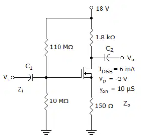
Referring to this figure, calculate Av for yos = 58uS.
a)
–7.29
b)
–8.55
c)
–8.05
d)
–7.50
92.
For what value of ID is gm equal to 0.5 gm0?
a)
0 mA
b)
0.25 IDSS
c)
0.5 IDSS
d)
IDSS
93.
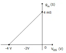
Referring to the following figure, calculate gm for VGSQ = –1.25 V.
a)
2 mS
b)
3.25 mS
c)
2.5 mS
d)
2.75 mS
94.
What is (are) the function(s) of the coupling capacitors C1 and C2 in an FET circuit?
a)
to isolate the dc biasing arrangement from the applied signal and load
b)
All of the above
c)
to create an open circuit for dc analysis
d)
to create a short-circuit equivalent for ac analysis
95.
There is a ________º phase inversion between gate and source in a source follower.
a)
None of the above
b)
0
c)
180
d)
90
96.
Which of the following is a required condition to simplify the equations for Zo and Av for the self-bias configuration?
a)
rd ≤ 10RD
b)
None of the above
c)
rd ≥ 10RD
d)
rd = RD
97.
MOSFETs make better power switches than BJTs because they have
a)
a positive temperature coefficient.
b)
lower turn-off times.
c)
all of the above
d)
lower on-state resistance.
98.
MOSFET digital switching is used to produce which digital gates?
a)
inverters
b)
all of the above
c)
NOR gates
d)
NAND gates
99.
Given IDSS=10mA. For midpoint biasing, ID would be
a)
5 mA
b)
2.5 mA
c)
10 mA
d)
7.5 mA
100.
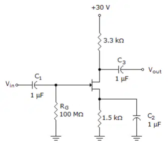
Refer to this figure. If ID = 4 mA, find the value of VGS.
a)
–6 V
b)
10.8 V
c)
–0.7 V
d)
6 V
101.
Which FET amplifier(s) has (have) a phase inversion between input and output signals?
a)
common-source
b)
All of the above
c)
common-drain
d)
common-gate
102.
The more horizontal the characteristic curves on the drain characteristics, the ________ the output impedance.
a)
same
b)
any of the above
c)
greater
d)
lesser
103.
For the fixed-bias configuration, if rd<10RD, then Zo=_______.
a)
RD
b)
RD||rd
c)
–gm(RD||rd)
d)
RG
104.
Which of the following is (are) related to depletion-type MOSFETs?
a)
VGSq can be negative, zero, or positive
b)
ID can be larger than IDSS.
c)
gm can be greater or smaller than gm0.
d)
All of the above
105.
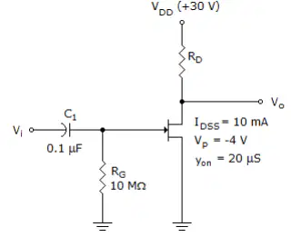
In the figure, determine the value for RD in Ω if the ac gain is 8
a)
1.65 k
b)
1.85 k
c)
2.08 k
d)
1.51 k
106.
What is the range of gm for JFETs?
a)
1 uS to 10 uS
b)
10000 uS to 100000 uS
c)
100 uS to 1000 uS
d)
1000 uS to 5000 uS
107.
Calculate gm and rd if yfs = 4 mS and yos = 15S.
a)
None of the above
b)
66.7 kΩ, 4 mS
c)
4 mS, 15 kΩ
d)
4 mS, 66.7 kΩ
108.
Input resistance of a common-drain amplifier is
a)
RG
b)
RIN(gate).
c)
RG + RIN(gate).
d)
RG || RIN(gate).
109.
E-MOSFETs are generally used in switching applications because
a)
of their very low input capacitance.
b)
of their high-frequency response capabilities.
c)
of their threshold characteristic (VGS(th)).
d)
of their power handling.
110.
A JFET cascade amplifier employs
a)
2 common-source amplifiers.
b)
1 common-gate and 1 common-drain amplifier.
c)
1 common-gate and 1 common-source amplifier.
d)
2 common-gate amplifiers.
111.
In a common-source amplifier, the purpose of the bypass capacitor, C2, is to
a)
keep the source effectively at ac ground.
b)
provide coupling to the input.
c)
provide coupling to the load.
d)
provide a dc path to ground.
112.
What is the ratio of the capacitive reactance XCS to the input resistance RI of the input RC circuit of a single-stage BJT amplifier at the low frequency cutoff?
a)
1.0
b)
0.50
c)
0.25
d)
0.75
113.
For which of the following frequency region(s) can the coupling and bypass capacitors no longer be replaced by the short-circuit approximation?
a)
High-frequency
b)
All of the above
c)
Low-frequency
d)
Mid-frequency
114.
What is the range of the capacitor Cds?
a)
0.1 to 1 F
b)
0.1 to 1 nF
c)
0.01 to 0.1 pF
d)
0.1 to 1 pF
115.
A 3-dB drop in hfe will occur at a frequency defined by ________.
a)
2
b)
1
c)
fB
d)
fα
116.
Which of the following elements is (are) important in determining the gain of the system in the high-frequency region?
a)
All of the above
b)
Wiring capacitances
c)
Interelectrode capacitances
d)
Miller effect capacitance
117.
For audio systems, the reference level is generally accepted as ________.
a)
1 mW
b)
1 W
c)
10 mW
d)
100 mW
118.
What is the normalized gain expressed in dB for the cutoff frequencies?
a)
–3 dB
b)
–6 dB
c)
+3 dB
d)
–20 dB
119.
Which of the following configurations does (do) not involve the Miller effect capacitance?
a)
Common-base
b)
Common-collector
c)
All of the above
d)
Common-emitter
120.
The ________-frequency response of a transformer-coupled system is calculated primarily by the stray capacitance between the turns of the primary and secondary windings.
a)
high
b)
low
c)
mid
d)
All of the above
121.
In the hybrid pi or Giacoletto model, which one of the following does rb include?
a)
All of the above
b)
Base contact
c)
Base bulk
d)
Base spreading resistance
122.
Which of the following statements is true for a square-wave signal?
a)
It is composed only of odd harmonics.
b)
The harmonics waveforms are also square waves.
c)
It is composed of both even and odd harmonics.
d)
It is composed only of even harmonics.
123.
In the input RC circuit of a single-stage BJT, by how much does the base voltage lead the input voltage for frequencies much larger than the cutoff frequency in the low-frequency region?
a)
About 0º
b)
About 90º
c)
45º
d)
None of the above
124.
What is the ratio of the output power to the input power at the cutoff frequencies in a normalized frequency response plot?
a)
1
b)
0.25
c)
0.707
d)
0.50
125.
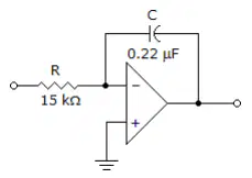
Refer to the given figure. This circuit is known as
a)
a differentiator.
b)
an integrator.
c)
a noninverting amplifier.
d)
a summing amplifier.
126.
Refer to the given figure at 125. A square-wave input is applied to this amplifier. The output voltage is most likely to be
a)
no output.
b)
a square wave.
c)
a sine wave.
d)
a triangle wave.
127.
If an op-amp comparator has a gain of 100,000, an input difference of 0.2 mV above reference, and a supply of 12 V, the output will be
a)
15 V
b)
20 V
c)
10 V
d)
12 V
128.
A comparator with a Schmitt trigger has
a)
a slow response.
b)
one trigger level.
c)
two trigger levels.
d)
a fast response.
129.
Refer to the given figure. If Vin = 5 V, the rate of change of the output voltage in response to a single pulse input is:
a)
15.2 mV/us
b)
15.2 V/us
c)
1.52 mV/us
d)
1.52 V/us
130.
In a flash A/D converter, the priority encoder is used to
a)
select the first input.
b)
select the highest value input.
c)
select the lowest value input.
d)
select the last input.
131.
To reduce the effects of noise resulting in erratic switching of output states of a comparator, you can use
a)
the lower trigger point.
b)
the upper trigger point.
c)
hysteresis.
d)
nonzero-level detection.
132.
What is (are) the necessary component(s) for the design of a bounded comparator?
a)
rectifier diodes
b)
zener diodes
c)
none of the above
d)
both of the above
133.
What type(s) of circuit(s) use comparators?
a)
summer
b)
averaging amplifier
c)
nonzero-level detector
d)
summer and nonzero-level detector
134.
Refer to the given figure. What is the output voltage?
a)
-0.5 V
b)
2 V
c)
0.5 V
d)
-2 V
135.
An integrator circuit
a)
uses a capacitor in its feedback circuit.
b)
uses an inductor in its feedback circuit.
c)
uses a resistor in its feedback circuit.
d)
uses a resistor in its feedback circuit or uses a capacitor in its feedback circuit
136.
________ is a mathematical process for determining the rate of change of a function.
a)
Comparatoring
b)
Summing
c)
Integration
d)
Differentiation
137.
Calculate the output voltage if V1 = –0.2 V and V2 = 0 V.
a)
-4 V
b)
-6.6 V
c)
0 V
d)
2 V
138.
How many op-amps are required to implement this equation?
a)
2
b)
3
c)
1
d)
4
139.
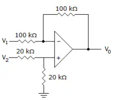
Determine the output voltage for this circuit with a sinusoidal input of 2.5 mV.
a)
-0.25 V
b)
0.125 V
c)
–0.125 V
d)
0.25 V
140.
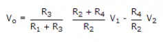
How many op-amps are required to implement this equation?
a)
1
b)
3
c)
2
d)
4
141.
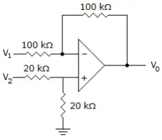
Determine the output voltage when V1 = –V2 = 1 V.
a)
0 V
b)
1 V
c)
-2 V
d)
2 V
142.
Calculate the cutoff frequencies of a bandpass filter with R1=R2=5 kΩ and C1=C2=0.1 uF.
a)
fOL = 636.6 Hz, fOH = 318.3 Hz
b)
fOL = 318.3 Hz, fOH = 636.6 Hz
c)
fOL = 636.6 Hz, fOH = 636.6 Hz
d)
fOL = 318.3 Hz, fOH = 318.3 Hz
143.
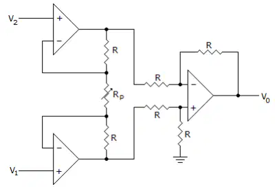
This circuit is an example of a(n)________.
a)
display driver
b)
instrumentation amplifier
c)
dc voltmeter
d)
none of the above
144.
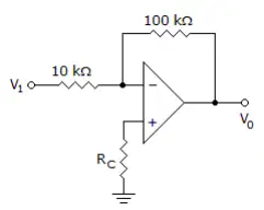
Calculate the input voltage for this circuit if Vo = –11 V. This circuit is an example of a(n)________.
a)
1.1 V
b)
1 V
c)
-1.1 V
d)
-1 V
145.
Calculate the cutoff frequency of a first-order low-pass filter for R1 = 2.5 kΩ and C1 = 0.05 uF.
a)
1.273 kHz
b)
12.73 kHz
c)
127.30 Hz
d)
127.3 kHz
146.
A filter that provides a constant output from dc up to a cutoff frequency and passes no signal above that frequency is called a ________ filter.
a)
bandstop
b)
high-pass
c)
bandpass
d)
low-pass
147.
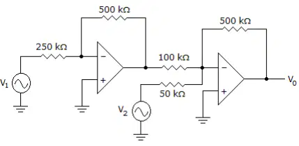
Calculate the output voltage Vo if V1 = –V2 = 300 mV.
a)
-6 V
b)
0 V
c)
6 V
d)
-8 V
148.
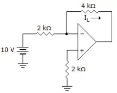
Calculate IL for this circuit.
a)
3 mA
b)
4 mA
c)
5 mA
d)
6 mA
149.
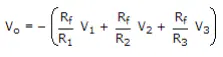
How many op-amps are required to implement this equation?
a)
1
b)
4
c)
3
d)
2
150.
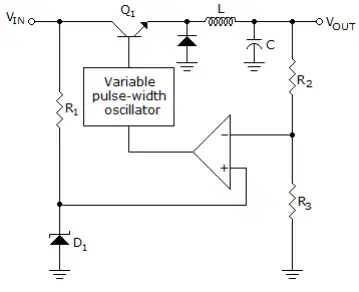
Refer to the given figure. This circuit operates at a ________ frequency, and its efficiency is ________.
a)
low, high
b)
low, low
c)
high, high
d)
high, low
151.
In which period is the capacitor filter discharged through the load in a full-wave rectifier?
a)
The time during the negative cycle
b)
The time during the positive cycle
c)
The time during which the diodes are not conducting
d)
The time during which the diode(s) is (are) conducting
152.
A voltage regulator with a no-load output dc voltage of 12 V is connected to a load with a resistance of 10Ω. If the load resistance decreases to 7.5Ω, the load voltage will decrease to 10.9V. The load current will be ________, and the percent load regulation is ________.
a)
1.2 A, 90.8%
b)
1.45 A, 90.8%
c)
1.2 A, 10.09%
d)
1.45 A, 10.09%
153.
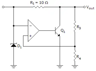
Refer to the given figure. This circuit is known as
a)
a step-down switching regulator.
b)
a shunt voltage regulator.
c)
a step-up switching regulator.
d)
a series-pass voltage regulator.
154.
If a peak rectified voltage for the full-wave filter circuit is 40 V, calculate the filter dc voltage if C = 75 F and load current is 40 mA.
a)
27.9 V
b)
40 V
c)
37.78 V
d)
32.12 V
155.
If the value of full-load voltage is the same as the no-load voltage, the voltage regulation calculated is ________ %, which is the best expected.
a)
0
b)
99
c)
100
d)
1
156.
A switching regulator that is configured as a voltage-inverter produces what type of output?
a)
an output that is a higher voltage than the input voltage
b)
an ac output with opposite phase to the input ac
c)
an ac output from a dc input voltage
d)
a dc output that is the negative of the dc input voltage
157.
For a full-wave rectifier with ac ripple at 120 Hz, the impedance of a capacitor can be calculated using XC = ________.
a)
0.785 ÷ C
b)
1.414 ÷ C
c)
1.3 ÷ C
d)
0.707 ÷ C
158.
In which of the following applications is a pulsating dc voltage suitable?
a)
Stereo system
b)
Computer
c)
Radio
d)
Battery charger
159.
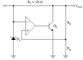
Refer to the given figure. If the output of the circuit were to be a short circuit, what power rating would R1 need to have?
a)
22.5 W
b)
10 W
c)
2.25 W
d)
5 W
160.
In a series regulator, what is the purpose of fold-back limiting?
a)
to provide more current in the case of a short circuit
b)
to limit output voltage if input voltage goes too high
c)
to bypass the pass-transistor, if the pass-transistor should fail
d)
to provide current up to a maximum, but drop current to a lower value when the output becomes shorted, to prevent overheating of the device
161.
Calculate the dc voltage across a 2-kΩ load for an RC filter section (R = 50Ω, C = 20uF). The dc voltage across the initial filter capacitor is Vdc = 50 V.
a)
42.78 V
b)
45.78 V
c)
48.78 V
d)
40.78 V
162.
In an improved shunt regulator, which of the following components sets the reference voltage?
a)
Transistor Q2
b)
Zener diode
c)
Transistor Q1
d)
RS
163.
How many terminals does a 7800 series IC regulator have?
a)
2
b)
3
c)
4
d)
none of the above
164.
What are the typical values of Vref and Iadj for the LM317 adjustable voltage regulator?
a)
1.5 V, 100 mA
b)
1.25 V, 100 μA
c)
1.0 V, 100 mA
d)
1.25 V, 10 mA
165.
Voltage regulation requires
a)
load and line regulation.
b)
only line regulation.
c)
only load regulation.
d)
a constant load.
166.
For what range of load current can voltage regulators be selected for operation?
a)
None of the above
b)
Hundreds of milliamperes to tens of amperes
c)
Hundreds of picoamperes to tens of milliamperes
d)
Hundreds of picoamperes to tens of nanoamperes
167.
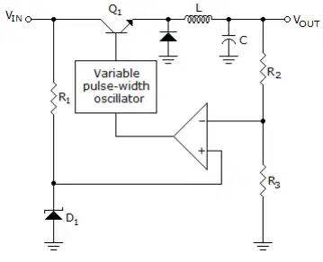
Refer to the figure at 150. The inductor and capacitor are used for
a)
turning on the pulse-width oscillator
b)
amplifying the error signal.
c)
filtering the dc pulse output.
d)
controlling the load current.
168.
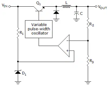
Refer to the figure at 150. If the output voltage tends to decrease due to an increase in load current, the transistor will conduct for ________ time each cycle.
a)
a shorter
b)
the same
c)
none of the above
d)
a longer
169.
For what range of fixed regulated voltages do the series 78xx regulators provide regulation?
a)
–5 V to +24 V
b)
+5 V to +24 V
c)
–5 V to –24 V
d)
None of the above
170.
In a series linear regulator, the control element is a(n) ________ in series with the load.
a)
capacitor
b)
resistor
c)
inductor
d)
transistor
171.
Filters with the ________ characteristic are useful when a rapid roll-off is required because it provides a roll-off rate greater than – 20/dB/decade/pole.
a)
Butterworth
b)
Elliptic
c)
Bessel
d)
Chebyshev
172.
A ________ filter rejects all frequencies within a specified band and passes all those outside this band.
a)
low-pass
b)
high-pass
c)
band-pass
d)
band-stop
173.
The bandwidth in a ________ filter equals the critical frequency.
a)
band-pass
b)
low-pass
c)
band-stop
d)
high-pass
174.
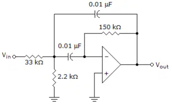
Refer to the given figure. The roll-off of this filter is about
a)
80 dB/decade.
b)
40 dB/decade.
c)
60 dB/decade.
d)
20 dB/decade.
175.
Which filter exhibits a linear phase characteristic?
a)
Butterworth
b)
Chebyshev
c)
All of the above
d)
Bessel
176.
The critical frequency is defined as the point at which the response drops ________ from the passband.
a)
-3 dB
b)
-40 dB
c)
-20 dB
d)
-6 dB
177.
Which filter has a maximally flat response?
a)
Butterworth
b)
Bessel
c)
Chebyshev
d)
All of the above
178.
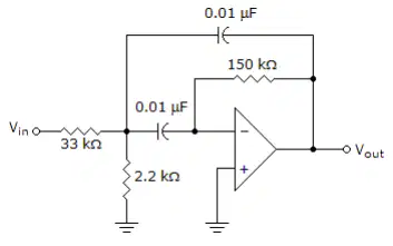
Refer to the given figure at 174. This is a ________ filter.
a)
band-stop
b)
high-pass
c)
low-pass
d)
band-pass
179.
One important application of a state-variable ________ filter with a summing amplifier is to minimize the 60 Hz "hum" in audio systems.
a)
band-stop
b)
band-pass
c)
low-pass
d)
high-pass
180.
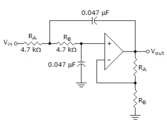
Refer to the given figure. RA = 2.2 k and RB = 1.2 k. This filter is probably a
a)
Elliptic type.
b)
Butterworth type.
c)
Chebyshev type.
d)
Bessel type.
181.
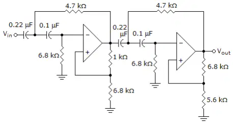
Refer to this figure. This filter has a roll-off rate of
a)
60 dB/decade.
b)
40 dB/decade.
c)
80 dB/decade.
d)
20 dB/decade.
182.
A third-order filter will have a roll-off rate of
a)
–40 dB/decade.
b)
–60 dB/decade.
c)
–20 dB/decade.
d)
–30 dB/decade.
183.
An AM demodulator can be implemented with a linear multiplier followed by a ________ filter.
a)
band-stop
b)
low-pass
c)
band-pass
d)
high-pass
184.
In order for a light ray to propagate along a fiber-optic cable, what must the relationship be between the angle of incidence and the critical angle?
a)
θi>θc
b)
θi<θc
c)
none of the above
d)
θi = θc
185.
Amplitude modulation is a ________ process.
a)
multiplication
b)
division
c)
exponential
d)
sum/difference
186.
What does VCO stand for?
a)
None of the above
b)
Voltage-Controlled Oscillator
c)
Visually-Controlled Organization
d)
Voltage-Centered Oscilloscope
187.
If a 1 MHz carrier is amplitude modulated with a 5 kHz audio signal, the upper-side frequency is ________ kHz.
a)
995
b)
1000
c)
none of the above
d)
1005
188.
Which of the following devices is unquestionably of the greatest interest today?
a)
SCS
b)
LASCR
c)
SCR
d)
GTO
189.
Determine RB1 for a silicon PUT if it is determined that h = 0.84, VP = 11.2 V, and RB2 = 5 kΩ.
a)
20.00 kΩ
b)
26.25 kΩ
c)
16.25 kΩ
d)
12.65 kΩ
190.
What is the typical value of the reverse resistance of SCRs in Ω?
a)
1 to 10
b)
100 k or more
c)
100 to 1 k
d)
1 k to 50 k
191.
The ISO-LIT Q1 16-pin Litronixopto-isolator DIP contains ________ opto-isolators.
a)
4
b)
6
c)
12
d)
8
192.
What is the frequency range of application of SCRs?
a)
About 10 kHz
b)
About 50 kHz
c)
About 250 kHz
d)
About 1 mHz
193.
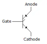
This symbol is an example of a(n) ________.
a)
GTO
b)
Diac
c)
SCS
d)
SCR
194.
Which of the following devices has nearly the same turn-on time as turn-off time?
a)
LASCR
b)
GTO
c)
SCR
d)
SCS
195.
Which of the transistors of an SCR are conducting when the SCR is fired and is in the conduction mode?
a)
Neither npn nor pnp
b)
pnp
c)
Both npn and pnp
d)
npn
196.
What is the maximum current (rms) rating for commercially available LASCRs today?
a)
3 A
b)
25 A
c)
15 A
d)
20 A
197.
Which of the following areas is (are) applications of an SCS?
a)
All of the above
b)
Pulse generators
c)
Counters
d)
Voltage sensors
198.
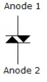
This symbol is an example of a(n) ________.
a)
SCS
b)
GTO
c)
SCR
d)
DIAC
199.
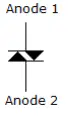
What is the typical value of the triggering anode gate for SCS devices?
a)
1.5 mA
b)
150 A
c)
15 A
d)
1 A
200.
This symbol is an example of a(n)________.
a)
SCS
b)
GTO
c)
DIAC
d)
SCR
100 %

