
Font size
 Worksheets
RAD 220 - Week 2 PREP
Total questions: 79
Worksheet time: 41mins
What does the aluminum or lead do in a cassette?
Protects the patient from scatter radiation
Protects the technologist from scatter radiation
Absorbs back scatter x-ray photons
Filters out low energy photons to improve spatial resolution
What is the anti-static material usually in PSP cassettes and what is its function?
Aluminum
Lead
Felt
Carbon Fiber
The layers of the imaging plate include:
1. Protective
2. Phosphor
3. Silver halide emulsion
4. Phosphor
5. Reflective
6. Conductive
7. TFT
8. Color
9. Support
10. Backing
1, 2, 3, 5, 6, 8, 9, 10
1, 2, 4, 5, 6, 8, 9, 10
2, 4, 5, 6, 7, 8, 9, 10
3, 5, 6, 8, 9, 10
What layer is a thin, tough, clear plastic that protects the phosphor layer?
Phosphor layer
Backing layer
Reflective layer
Protective layer
What is the phosphor layer made of?
Cesium Iodide crystals in a structured configuration
Gadolinium Oxysulfide in turbid formation
Photostimulable phosphor that is part of the barium fluorohalide family
Silver Halide crystals
This layer sends light in a forward direction when released in the reader. May be black to reduce the spread of stimulating light and the escape of emitted light. Some detail is lost in this process.
Phosphor layer
Backing layer
Protective layer
Reflective layer
This materials absorbs and reduces static electricity in PSP cassettes.
Conductive layer
Reflective layer
Phosphor layer
TFT layer
This layer absorbs the stimulating light but reflects emitted light.
Color layer
Phosphor layer
Where is the color layer located?
Between the protective and phosphor layers
Between the active and support layers
Between the reflective and conductive layer
Between the phosphor and reflective layer
What layer gives the imaging plate strength?
Reflective layer
Backing layer
Conductive layer
Support layer
In _____ imaging, the remnant beam interacts with electrons in the barium fluorohalide crystals contained within the plate. The stimulated electrons in the crystals are trapped in the phosphor center.
Film/Screen
PSP
Direct Digital
Indirect Digital
What are the two types of PSP readers?
Point scan
Field scan
Flat bed scan
Line scan
What are the two scan directions of a PSP reader?
Axial
Fast
Rapid
Slow
This type of scan describes the movement of the plate through the reader AKA translation or subscan direction.
Fast
Slow
Direct
Indirect
This is the movement of the laser across the PSP IP.
Slow
Raster
Fast
Scaling
In a PSP reader, what does the photodetector do?
Amplifies the light and sends it to an ADC
Captures the x-ray photons and converts them into visible light
Captures electrons and stores them for transmission and image production
Stops the x-ray exposure when a sufficient dosage is reached
Why would we increase kVp?
To promote photoelectric absorption
To increase patient exposure
To decrease mAs
To prevent repeat imaging
What are the primary grid selection factors?
Weight
Frequency
Ratio
Focus
This is a wavy artifact that causes grid lines running parallel to the laser scanning motion.
Waters effect
Moire effect
Linear flux effect
Off focus effect
The relationship between the height of the lead strips and the space between them is grid ____.
Frequency
Ratio
Focus
Cutoff
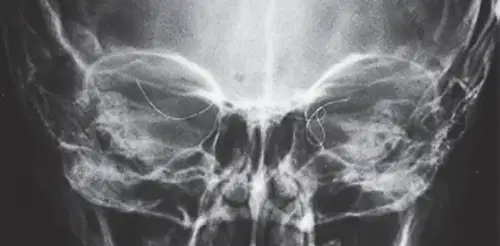
What is the most likely cause of the artifact in this image?
Processing error
Moire effect from incorrect grid frequency
Static electricity
Hair stuck between cassette and IP
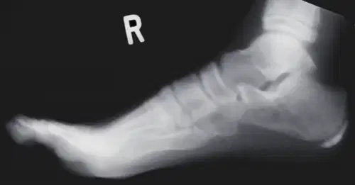
What is the error with this image?
Double exposure
Motion
Poor IP contact
Static electricity
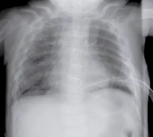
What type of error is exhibited in this image?
Motion
Double exposure
Rescaling error
Histogram error
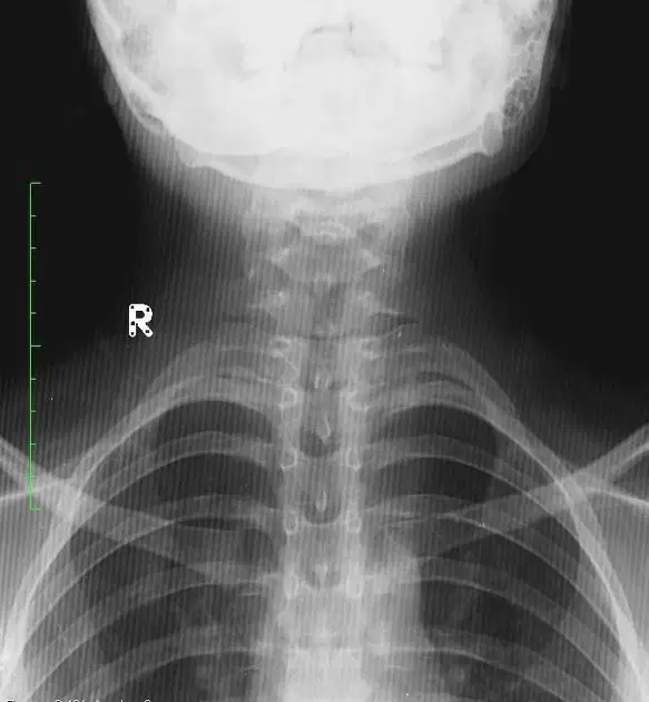
What type of artifact is seen in this image?
Off focus grid
Off level grid
Moire effect
Incorrect grid ratio
The oldest indirect conversion digital radiography systems used what to acquire the digital image?
CMOS
TFT
CCD
Intensifying screens
Which of the following is not considered a scintillator?
Gd2O2S
CsI
A-Se
Which of the following is used as a photodetector?
A-Se
CsI
A-Si:H
Gd2O2S
Which of the following are not found in an AMFPI?
a-Si TFT with CsI
a-Se with TFT
PSP
Scintillator
Which detector converts x-ray energy directly into electrons?
a-Si:H
photodetector
a-Se
CsI
A Gd2O2S scintillator is known as what type of phosphor?
Structured
Turbid
Rigid
Amorphous
True or False: Gain calibration will remove inherent detector artifacts from an image.
True
False
True or False: Offset correction is used to remove inherent signal that remains in a detector.
True
False
What can be done to decrease the change of having image lag occur in the next image?
Decrease the amount of time between exposures
Use a higher than normal exposure to adequately saturate the detector
Increase the amount of time between exposures
Reduce collimation so that more of the field is exposed
Which of the following requires capacitor as the storage element?
a-Se
Gd2O2S
PSP
CsI
A material that absorbs x-ray energy and emits part of that energy as visible light is called:
Diode
Scintillator
TFT
Cathode
Digital image receptors are more sensitive to:
Scatter and background radiation
Fluorescent lights
Free electrons
Free radicals
In digital radiography inappropriate collimation causes:
A fogged image
Pixel unresponsiveness
DICOM incompatibility
Histogram analysis error
The appearance of digital images on technologists' monitors is:
The same as on radiologists' monitors
Substantially better than on radiologists' monitors
Not as good as on radiologists' monitors
If the exposure field is not accurately recognized, the histogram will contain data:
Outside the exposure field, narrowing the histogram
Inside the exposure field, widening the histogram
Outside the exposure field, widening the histogram
Inside the exposure field, narrowing the histogram
Receptor exposure may be defined as:
Amount of remnant radiation striking the image receptor
Dose area product (DAP)
DQE
Differences in dark areas on a radiographic image
Barcodes on the back of the IP:
Identify the cassette and link it to a specific patient exam/projection
Identify cassettes used within a specific radiology department and are linked to a specific IP reader
Identify the technologist that performed the imaging exam
Are not relevant to imaging studies
The photoconductor in a detector:
Absorbs light photons and emits light
Absorbs electrons and emits light
Converts light into an electrical signal
Absorbs x-rays and produces and electrical charge
Dark line artifacts on images can be caused by:
a mAs that is too high
a kVp that is too high
grid lines
hair or dust in the cassette
True or False: Radiologic technologists are responsible for servicing/cleaning/maintenance of IP readers and their components.
True
False
What layer 'traps' the excited electrons in a PSP plate during x-ray imaging?
Protective layer
Active layer
Passive layer
Conductive layer
The laser light that reads PSP phosphors is:
Blue
Green
Red
Purple
LASER stands for:
Let's All Stop Emitting Radiation
Light Analog Signal Emitter Region
Light Amplification by Stimulated Emission of Radiation
Light Amplifier and Signal Extractor Rig
Image lag results when:
The phosphors in an IP fail to respond to an x-ray exposure
Processing delays length image output time
An image is taken with a digital detector system before the detector releases all of the previous exposure signal
A radiologic technologist takes too long to process an IP exposure
More pixels + fixed field of view =
lower resolution
no correlation between pixels and field of view
higher resolution
lower contrast
In PSP imaging, a thinner phosphor layer gives _____ resolution, and a thicker phosphor layer gives _____ resolution.
lower; higher
contrast; spatial
higher; lower
no; higher
True or False: CR and PSP are the same imaging technology.
True
False
The photomultiplier tube in a PSP reader:
records the blue light that is emitted from the phosphor layer in the IP
converts x-rays to light
converts x-rays to electrons
scans the IP
What prime factor affects the penetrability of the x-ray beam and is adjusted according to the body tissue we're imaging?
mAs
SID
kVp
Grid factor
X-ray beam quality refers to ____, and x-ray beam quantity refers to ____.
SID; kVp
mAs; kVp
kVp; mAs
density; contrast
The wavy linear artifact in this image is caused by grid lines running in parallel to the laser scanning direction and is also called:
hair in the IP cassette
backscatter
quantum mottle
Moire effect
The higher the grid frequency;
the more positioning latitude that grid offers
the less positioning latitude that grid offers
the lower the patient dose
the lesser the mAs needed
Grid ratio = ___/___
length of lead strips; width of lead strips
distance between lead strips; height of lead strips
height of lead strips; distance between lead strips
kVp; mAs
True or False: CCD technology quantum efficiency can be measured by how efficiently it collects light and the signal created in the CCD chip.
True
False
The materials used for detecting x-ray signal and the sensors for recognizing that signal in FPD technology are:
temporarily enclosed inside a rigid protective casing
permanenty enclosed inside a rigid protective casing
should be removed prior to processing
require chemical processing and a dark room
The active layer in PSP imaging is composed of:
Barium sulfate
Barium Platinocyanide
Barium fluorohalide doped with Europium
Cesium Iodide
Which of the following are true of the PSP plate erasure?
1. Can be initiated by manually selecting the proper eraser method
2. Should be performed after every PSP plate processing or on a weekly basis
3. Should be performed in a dark room
4. Is performed by flooding the PSP plate with bright white light
5. Is accomplished by the laser scanning sequence in the IP reader
1, 2, and 5
1, 2, 3, and 4
1, 2, and 4
1, 2, and 5
If an IP cassette is imaged backwards:
there will be no issue. IPs are reversible and can be used in either orientation.
Metallic (i.e. radiopaque) latch-shaped artifacts will result on the processed image
'Lightning bolt' shaped artifacts will be visible on the final processed image
Dark linear artifacts will be visible on the final image
Quantum mottle results from:
too low kVp setting
too low mAs setting
too low SID
too high kVp setting
When a capacitor is used as a storage element, the absorbing materials that can be used include:
Scintillator
a-Si
a-Se
Photoconductor
True or False: A CCD converts light into x-ray photons for image processing.
True
False
The number of electron/hole pairs in CCD technology is related to:
the amount of reflected light
the amount of electric charge
the amount of incident x-rays
the amount of light absorbed
What layer in a CCD chip contains the electron gates?
silicon substrate
polysilicon layer
silicon dioxide layer
All of the above
What layer in a CCD chip acts as an insulating layer?
monosilicon layer
polysilicon layer
silicon dioxide layer
silicon substrate layer
What type of light is emitted from the phosphor layer in IP processing after scanning with the laser beam?
Purple
Infrared
Red
Blue
Which of the following factors are important when selecting a PSP imaging cassette?
Type
Shape
Grid
Size
A ____ acts as a receptor that senses light generated in a scintillator and then sends the light to capacitors in the pixel that converts light to an electrical charge.
CMOS
CCD
IP
CR
What type of light is used to erase IPs?
Infrared
Fluorescent/white
Red
Helium neon
The four common types of artifacts include:
1. Image artifacts
2. Electrical artifacts
3. Plate reader artifacts
4. Image processing artifacts
5. Printer artifacts
6. Phosphor artifacts
1, 2, 3, and 4
1, 3, 4, and 5
1, 2, 3, and 6
1, 3, 5, and 6
Overexposure has what effect on image contrast?
Increases
No effect
Reduces
A lack of light photons from the scintillator causes what kind of noise?
Amplification
Statistical
Fog
Scatter
CMOS systems were developed by NASA and uses a _____.
Photodetector
Scintillator
CCD
PSP
Between CCD and CMOS, which is more susceptible to noise?
CCD
CMOS
With which system is the fill factor greater?
CCD
CMOS
The three types of noise associated with CCD include:
statistical
dark current
amplification
anatomical

